Wafer bonding misalignment reduction

a technology of misalignment and bonding, applied in the field of wafer bonding, can solve the problems of increasing the limitations of scaling through silicon vias (tsvs) and associated tsv landing pad areas, and achieve the effect of reducing misalignmen

Inactive Publication Date: 2014-12-02
GLOBALFOUNDRIES INC
View PDF10 Cites 15 Cited by
  • Summary
  • Abstract
  • Description
  • Claims
  • Application Information

AI Technical Summary

Benefits of technology

[0006]Another method for wafer bonding includes measuring grid distortion for a mated pairing of wafers to be bonded to determine if misalignment exists between the wafers; during processing of subsequent wafers, making grid distortion measurements continuously to provide feedback for making lithographic magnification offset adjustments to minimize misalignment; and bonding the subsequent wafers.

Problems solved by technology

Mismatches between these layers increase limitations to scaling through silicon vias (TSVs) and associated TSV landing pad areas.

Method used


Image

  • Wafer bonding misalignment reduction
  • Wafer bonding misalignment reduction
  • Wafer bonding misalignment reduction

Examples


Embodiment Construction

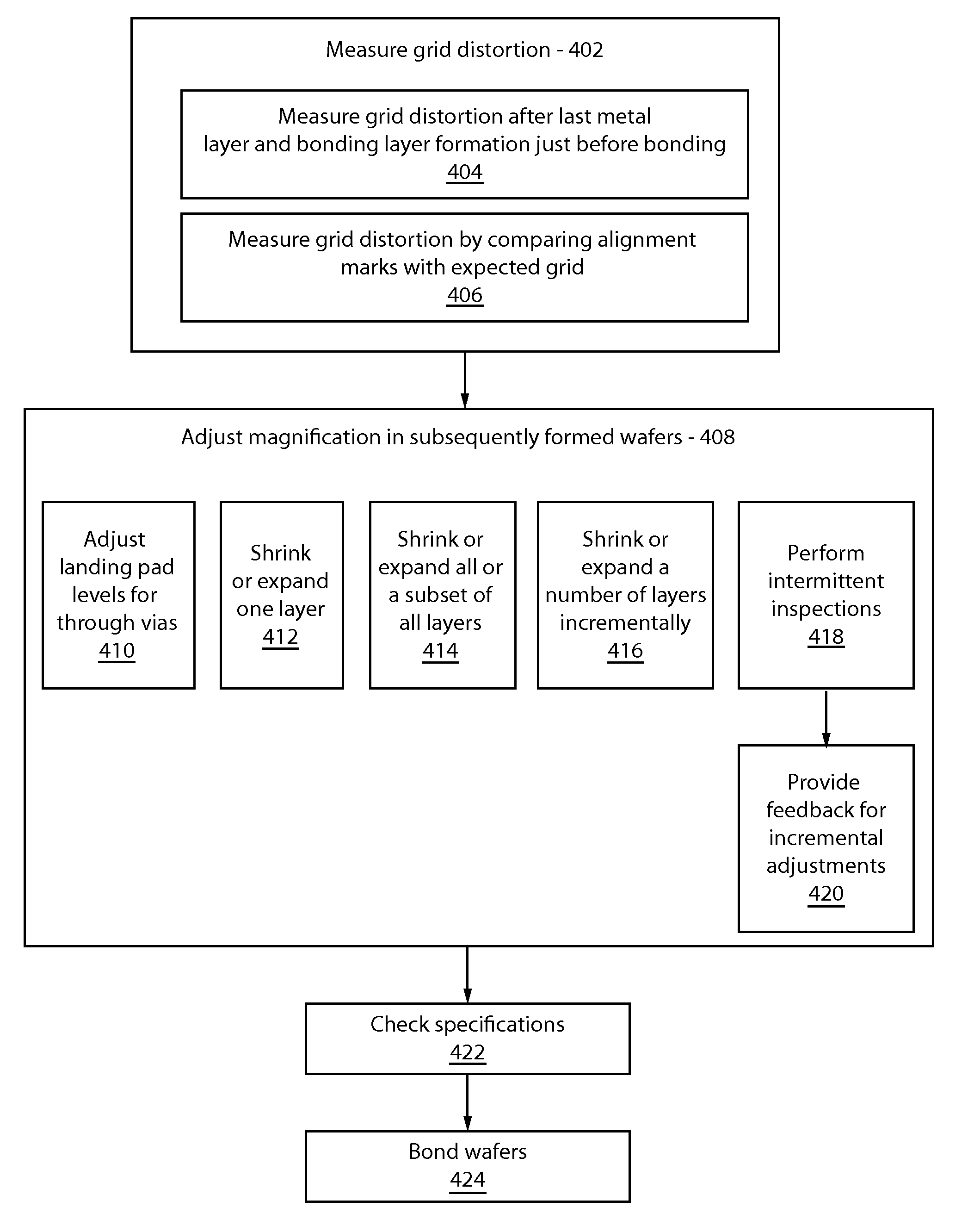
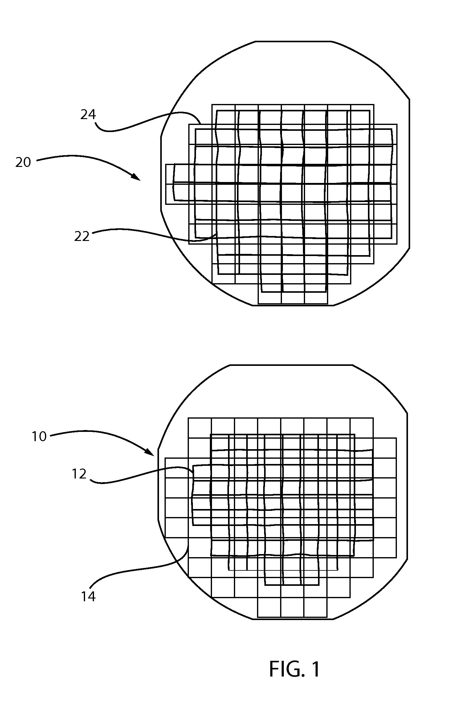
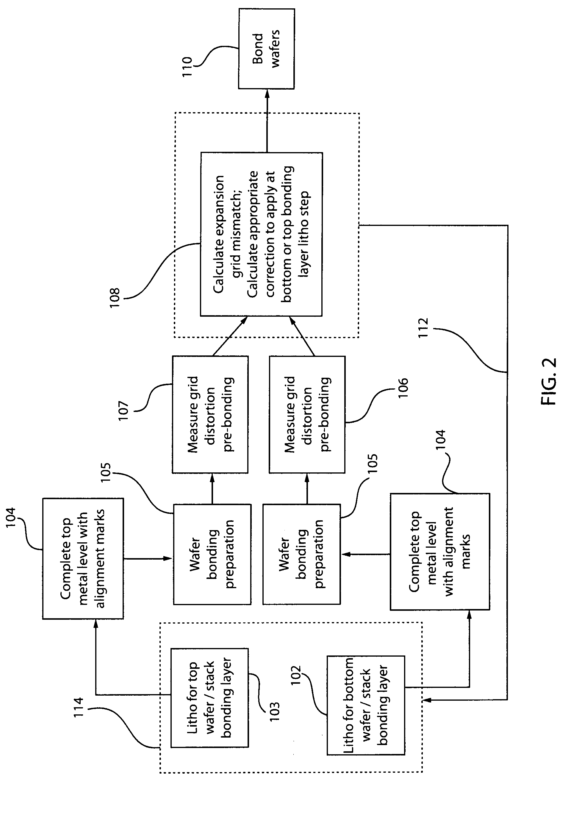
[0018]In accordance with the present principles, magnification corrections are employed as needed to different levels of wafers to be bonded to improve wafer alignment. Bonding layer preparation is executed, which may include preparing layers for bonding. At this point, grid distortion is measured before wafer bonding to establish if there is a magnification mismatch between top and bottom wafers. During processing or an integration setup, grid distortion is measured, e.g., by aligning mark positions against an expected grid.

[0019]Based on learning, shrinking or expansion is performed on lithographic exposure for one or both of the bonding layers as needed or as possible. In one embodiment, the grid distortion measurements may continuously be employed as feedback to control lithographic magnification to minimize misalignment. The present principles address the issues associated with lithographic magnification corrections as needed for the levels of the wafers to be bonded.

[0020]It i...


PUM


Abstract

A method for wafer bonding includes measuring grid distortion for a mated pairing of wafers to be bonded to determine if misalignment exists between the wafers. During processing of subsequent wafers, magnification of one or more lithographic patterns is adjusted to account for the misalignment. The subsequent wafers are bonded with reduced misalignment.

Description

BACKGROUND[0001]1. Technical Field[0002]The present invention relates to wafer bonding, and more particularly to methods for improving alignment between wafers to be bonded.[0003]2. Description of the Related Art[0004]Bonding layer grid mismatch between top and bottom wafers can be observed prior to wafer bonding. Mismatches between these layers increase limitations to scaling through silicon vias (TSVs) and associated TSV landing pad areas. Such differences can occur during lithographic processing or, more likely, due to bonding preparation, especially if the wafers are quite different (e.g., single versus stack, pattern loading, etc.).SUMMARY[0005]A method for wafer bonding includes measuring grid distortion for a mated pairing of wafers to be bonded to determine if a magnification mismatch exists between the wafers. During processing of subsequent wafers, magnification of one or more lithographic patterns is adjusted to account for the magnification mismatch. The subsequent wafer...

Claims


Application Information

Patent Timeline
Patent Type & Authority Patents(United States)
IPC IPC(8): H01L21/00H01L23/00H01L21/30H01L21/66
CPCH01L22/12H01L24/80H01L2224/8313H01L2924/3511H01L24/32H01L24/81H01L24/92H01L2224/8013H01L2224/94H01L2224/81908H01L2224/80908H01L2224/83908H01L23/544H01L24/13H01L24/16H01L2224/16145H01L2224/80896H01L2225/06513H01L2223/54426H01L2224/9202H01L24/29H01L2225/06541H01L2224/0401H01L2224/2919H01L2224/08145H01L24/83H01L2224/131H01L24/94H01L2224/32145H01L2224/8113H01L25/0657H01L2224/80H01L2224/81H01L2224/83H01L2924/014
Inventor HUBBARD, ALEX R.LA TULIPE, JR., DOUGLAS C.SKORDAS, SPYRIDONWINSTEL, KEVIN R.
Owner GLOBALFOUNDRIES INC
Why Eureka
Try Eureka