Eureka AIR delivers breakthrough ideas for toughest innovation challenges, trusted by R&D personnel around the world.

Liquid crystal display structure

Active Publication Date: 2003-04-24
AU OPTRONICS CORP
View PDF12 Cites 11 Cited by
  • Summary
  • Abstract
  • Description
  • Claims
  • Application Information

AI Technical Summary

Benefits of technology

[0009] Accordingly, one object of the present invention is to provide a liquid crystal display structure capable of minimizing liquid crystal misalignment in the liquid crystal layer and liquid crystal cell gap non-uniformity problem.
[0010] A second object of this invention is to provide a liquid crystal display structure having excellent legibility and display efficiency under any surrounding lighting levels.
[0011] A third object of this invention is to provide a liquid crystal display structure having much better legibility and display efficiency under any lighting levels and less misalignment in a liquid crystal layer and reduced liquid crystal cell gap non-uniformity problems.
[0012] To achieve these and other advantages and in accordance with the purposes of the invention, as embodied and broadly described herein, the invention provides three liquid crystal display (LCD) structures which can improve the viewing performances of the LCDs.
[0015] Since a material film having a non-planar surface is an essential aspect of the LCD structure but may lead to liquid crystal misalignment and liquid crystal cell gap non-uniformity problems, a dielectric layer having a relatively planar upper surface is formed over the material film. The dielectric layer can be a color filter layer or a transparent insulating layer. A transparent conductive layer is later formed over the dielectric layer. With this structural arrangement, the liquid crystal layer has a uniform thickness throughout and hence problems caused by having a non-planar reflection layer are avoided.
[0016] To achieve these and other advantages and in accordance with the purpose of the invention, as embodied and broadly described herein, the invention provides a liquid crystal display (LCD) structure, which utilizes the portions of the reflector surface which contributes to the useful reflected lights and convert the nonuseful parts of the reflector into transmissive region by removing the reflectors, the efficiency of the LCD can be significantly improved. The LCD structure is a transflective (transmissive / reflective) type of liquid crystal display. One pixel portion of the second LCD structure includes a first substrate panel, an organic insulating layer, a plurality of conformal transparent conductors, a plurality of conformal reflectors, a thin film transistor, a second substrate panel, a second transparent conductive layer, a color filter layer, a liquid crystal layer and a back lighting system.

Problems solved by technology

Due to the non-planarity of the reflective electrode 22 surface, liquid crystal misalignment and non-uniformity of liquid crystal cell gap inside the pixels can be detrimental to the display performance.
Ultimately, quality of the liquid crystal display product is compromised.
When the reflective angle of the light beam greater or less than this range, the viewing condition is poor for the viewer.
Hence, reflected lights at various angles outside the range are not effective for viewing.

Method used


Image

  • Liquid crystal display structure
  • Liquid crystal display structure
  • Liquid crystal display structure

Examples


Embodiment Construction

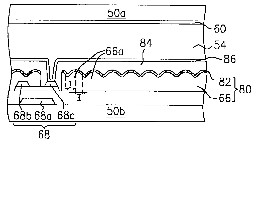
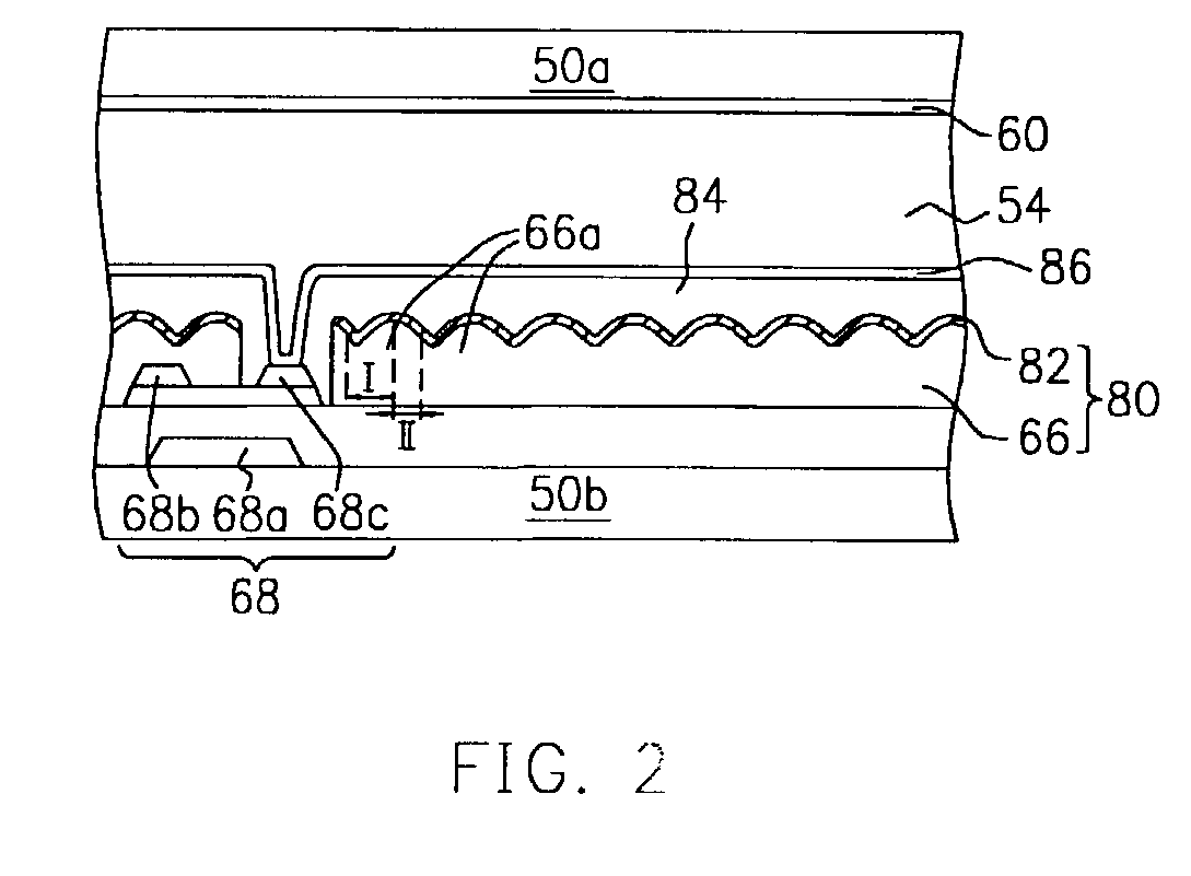
[0029] Reference will now be made in detail to the present preferred embodiments of the invention, examples of which are illustrated in the accompanying drawings. Wherever possible, the same reference numbers are used in the drawings and the description to refer to the same or like parts.

[0030] FIG. 2 is a schematic cross-sectional view showing a first type of one pixel portion of a liquid crystal display structure according to a first preferred embodiment of this invention. A first glass panel or a first substrate panel 50b and a second glass panel or a second substrate panel 50a (the first glass panel 50b is the lower glass panel and the second glass panel 50b is the upper glass panel) are provided. The first glass panel 50b and the second glass panel 50a together enclose all the component layers, including layers such as a liquid crystal layer 54 and a color filter layer 84, of a liquid crystal display (LCD). A quarter wave plate, a phase compensation plate and a polarizer compos...


PUM


Abstract

A liquid crystal display structure includes a first substrate panel, a second substrate panel, and a liquid crystal layer disposed between the first substrate panel and the second substrate panel. Pixel portions are formed by respective electrodes for applying a voltage to the liquid crystal layer. The pixel portions include a transparent substrate panel, an organic insulating layer, a patterned reflective layer, a dielectric layer, a transparent conductive layer and a thin film transistor. The organic insulating layer is formed over the transparent substrate panel. The patterned reflective layer is formed over the organic insulating layer exposing a portion of the organic insulating layer. The dielectric layer is formed over the patterned reflective layer. The dielectric layer has a smooth upper surface. The transparent conductive layer is over the dielectric layer. The transparent conductive layer is connected to the thin film transistor so that the thin film transistor can drive the transparent conductive electrode.

Description

[0001] This application claims the priority benefit of Taiwan application serial no. 90126138, filed Oct. 23, 2001.BACKGROUND OF INVENTION[0002] 1. Field of Invention[0003] The present invention relates to a liquid crystal display (LCD) structure. More particularly, the present invention relates to a reflective and transflective type of liquid crystal display or liquid crystal display structure with excellent legibility and display efficiency.[0004] 2. Description of Related Art[0005] In recent years, the applications of liquid crystal display (LCD) are far and wide following full integration with various electronic device packages. Functional capacity and complexity of typical LCD such as liquid crystal monitors and PDAs also expand with time. In general, LCD devices may be categorized into three major types, namely, the reflective type, the transmissive type and the transflective type.[0006] FIG. 1 is a cross-sectional view of one conventional pixel portion of the transflective li...

Claims


Application Information

Patent Timeline
IPC IPC(8): G02F1/1335
CPCG02F1/133555G02F2001/136222G02F2001/133357G02F1/136227G02F1/133357G02F1/136222
Inventor LUO, FANG-CHENCHANG, WEI-CHIH
Owner AU OPTRONICS CORP
Why Eureka
Eureka Blog
Learn More