Touch sensing substrate and method of manufacturing the same

a technology of touch sensing and substrate, which is applied in the direction of instruments, solid-state devices, radio-controlled devices, etc., can solve the problems of non-uniform side profiles, source and drain electrodes may be short circuits, etc., and achieve the effect of improving process reliability of source and drain electrodes

Inactive Publication Date: 2014-12-02
SAMSUNG DISPLAY CO LTD
View PDF32 Cites 2 Cited by
  • Summary
  • Abstract
  • Description
  • Claims
  • Application Information

AI Technical Summary

Benefits of technology

[0009]Exemplary embodiments of the present invention provide a touch sensing substrate capable of improving process reliability of source and drain electrodes.
[0014]According to the present invention, the source and drain electrodes are connected to the source and drain connection electrodes through the contact hole, so that the source and drain electrodes may be prevented from forming a short circuit. In addition, the source and drain electrodes are patterned using two metal layers having etching selectivity different from each other, so that a manufacturing process may be simplified.

Problems solved by technology

The active pattern has a non-uniform side profile due to the first photolithography process, which may cause defects.
For example, defects of the non-uniform side profile may include a tip which remains from the un-etched insulating layer covering the active pattern, a stringer due to an un-covered active pattern by an etch stopping layer, etc.
Another defect may be that because the source and drain electrodes are formed after forming the active pattern, the source and drain electrodes may be a short circuit due to the non-uniform side profile of the active pattern.

Method used


Image

  • Touch sensing substrate and method of manufacturing the same
  • Touch sensing substrate and method of manufacturing the same
  • Touch sensing substrate and method of manufacturing the same

Examples


Embodiment Construction

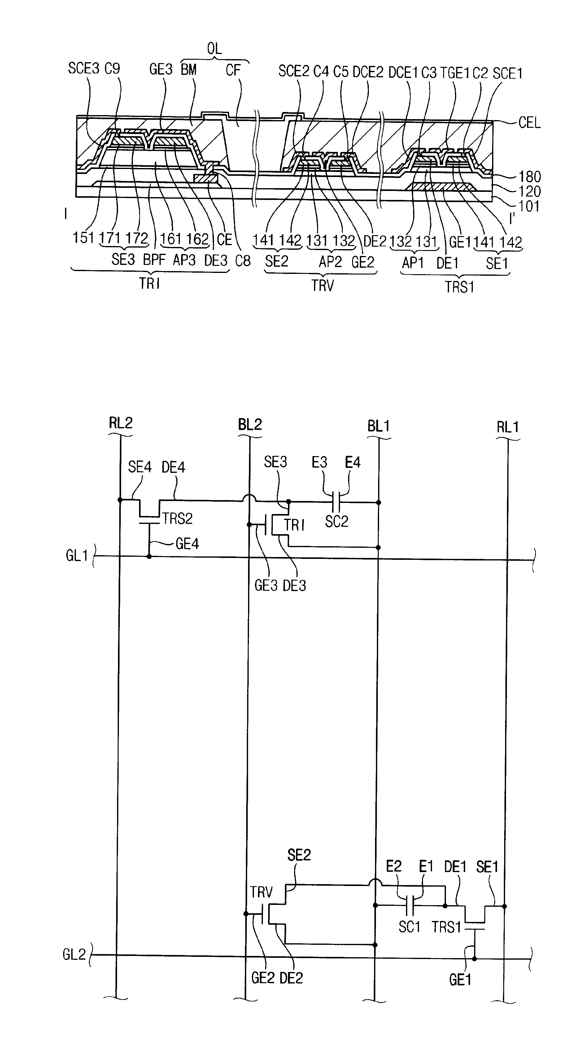
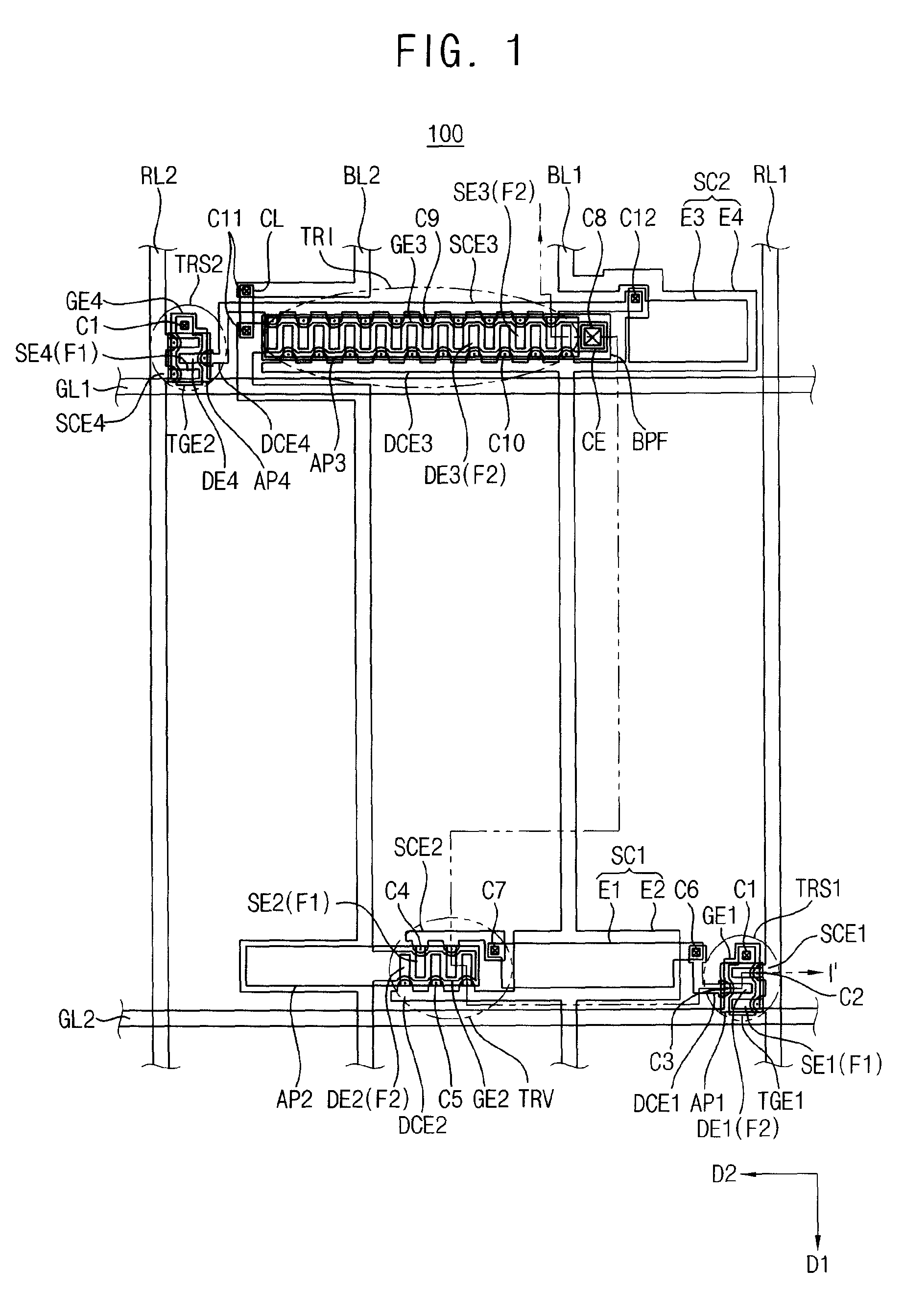
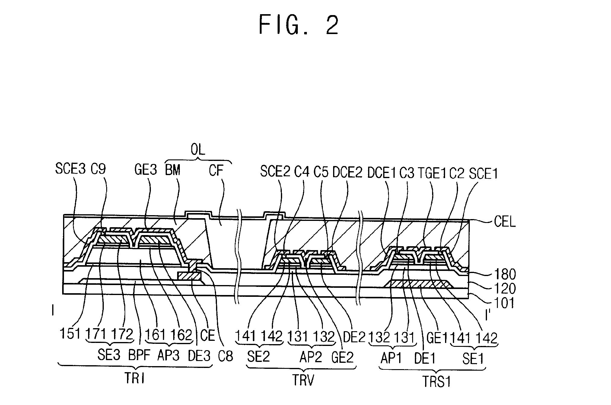
[0024]Hereinafter, the present invention will be explained in detail with reference to the accompanying drawings.

[0025]It will be understood that, although the terms first, second, third etc. may be used herein to describe various elements, components, regions, layers and / or sections, these elements, components, regions, layers and / or sections should not be limited by these terms. These terms are only used to distinguish one element, component, region, layer or section from another region, layer or section. Thus, a first element, component, region, layer or section discussed below could be termed a second element, component, region, layer or section without departing from the teachings of the present invention. It will be understood that when an element or layer is referred to as being “on” or “connected to” another element or layer, it can be directly on or directly connected to the other element or layer, or intervening elements or layers may be present. In contrast, when an eleme...


PUM


Abstract

A touch sensing substrate includes a substrate, a first light sensing element, a second light sensing element and a first bias line. The first light sensing element includes a first gate electrode, a first active pattern overlapping with the first gate electrode, a first source electrode partially overlapping with the first active pattern and a first drain electrode partially overlapping with the first active pattern. The second light sensing element includes a second gate electrode, a second active pattern overlapping with the second gate electrode, a second source electrode partially overlapping with the second active pattern and a second drain electrode partially overlapping with the second active pattern. The first bias line is connected to the first and second gate electrodes.

Description

CROSS-REFERENCE TO RELATED APPLICATION[0001]This application claims priority from and the benefit of Korean Patent Application No. 2011-6360, filed on Jan. 21, 2011, which is hereby incorporated by reference for all purposes as if fully set forth herein.BACKGROUND OF THE INVENTION[0002]1. Field[0003]Example embodiments of the present invention relate to a touch sensing substrate and a method of manufacturing the touch sensing substrate. More particularly, example embodiments of the present invention relate to a touch sensing substrate capable of improving process reliability and a method of manufacturing the touch sensing substrate.[0004]2. discussion of the Background[0005]In the field of liquid crystal display (LCD) panels, a touch display panel having an input function in addition to displaying an image has been developed with the touch display panel including a sensing element to sense a touch position. Specifically, the touch display panel may include a first substrate on which...

Claims


Application Information

Patent Timeline
Patent Type & Authority Patents(United States)
IPC IPC(8): G06F3/042H01L27/32G06F3/041
CPCG06F3/042G06F3/0412G06F2203/04103
Inventor YEO, YUN-JONGCHO, BYEONG-HOONJEONG, KI-HUNCHIN, HONG-KEEBANG, JUNG-SUKKIM, WOONG-KWONKIM, SUNG-RYULKIM, HEE-JOONKIM, DAE-CHEOLHAN, KUN-WOOK
Owner SAMSUNG DISPLAY CO LTD
Why Eureka
Try Eureka