Structured placement of latches/flip-flops to minimize clock power in high-performance designs

a latch and latch-flip technology, applied in the direction of instruments, computing, electric digital data processing, etc., can solve the problems of large number of cells, difficult to achieve physical design without the aid of computers, and complex connections between cells, so as to minimize the total length of the overall layout and optimize latch placement within the cluster

Inactive Publication Date: 2015-02-10
GLOBALFOUNDRIES INC
View PDF10 Cites 18 Cited by
  • Summary
  • Abstract
  • Description
  • Claims
  • Application Information

AI Technical Summary

Benefits of technology

[0010]The present invention is generally directed to a method of designing a layout for a cluster of latches in a common clock domain of an integrated circuit, by determining a shape of the cluster in a preliminary layout, including an aspect ratio of the shape, generating a template for placement of the latches in conformity with the shape of the cluster in the preliminary layout, and placing the latches in the template around a local clock buffer. The cluster of latches can be identified based on layout features in a placement image of the preliminary layout. The template preferably has an aspect ratio that is approximately equal to the aspect ratio of the shape of the cluster, but the latch placement may be constrained by the clock routing topology. In the illustrative implementation, latches are placed around the local clock buffer in order based on latch size, from largest latch first to smallest latch last. Latch placement within a cluster can be further optimized by swapping one of the latches with another to minimize total wirelength of the overall layout.

Problems solved by technology

An IC may include a very large number of cells and require complicated connections between the cells.
Due to the large number of components and the details required by the fabrication process for very large scale integrated (VLSI) devices, physical design is not practical without the aid of computers.
While current placement techniques provide adequate placement of cells with regard to their data interconnections, there is an additional challenge for the designer in constructing a clock network for the cells and this challenge is becoming more difficult in the context of modern technologies such as those used to design low-power integrated circuits in the 65-nanometer technology node and below.
Low power circuits (e.g., around 20 watts or less for microprocessor chips) are becoming more prevalent due to power consumption problems.
In particular, power dissipation has become a limiting factor for the yield of high-performance circuit designs (operating at frequencies around 1 gigahertz or more) fabricated in nanometer-scale technologies.

Method used


Image

  • Structured placement of latches/flip-flops to minimize clock power in high-performance designs
  • Structured placement of latches/flip-flops to minimize clock power in high-performance designs
  • Structured placement of latches/flip-flops to minimize clock power in high-performance designs

Examples


Embodiment Construction

)

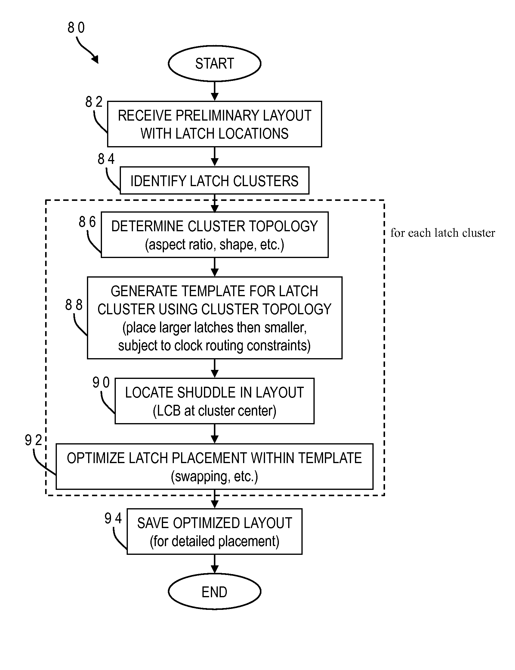
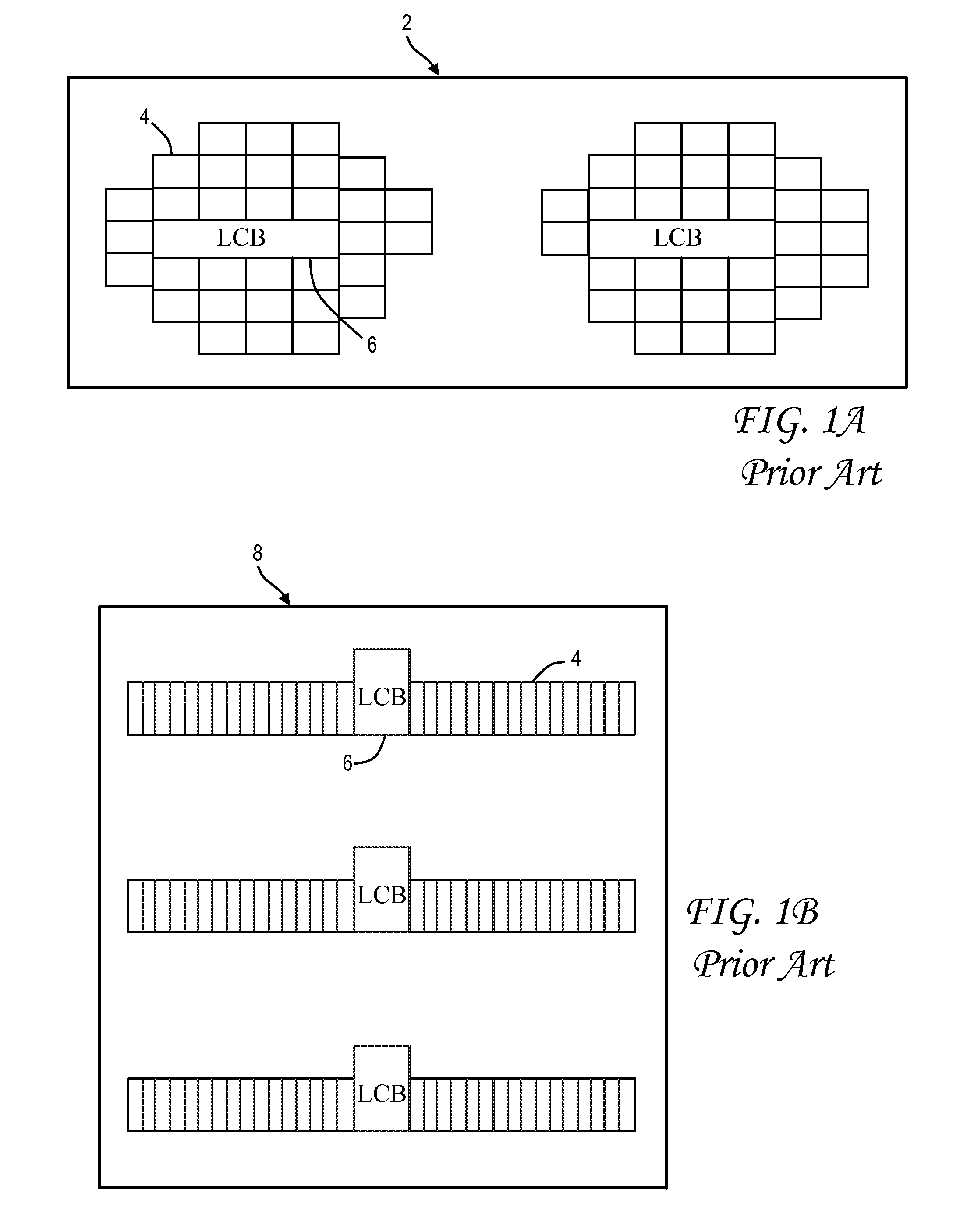
[0019]While existing approaches to latch clustering have certain benefits, they all still suffer other disadvantages. For example, while the huddle placement approach is more compact and is easily legalized, it places the latches around an LCB in an amorphous manner with no notion of a structure or regularity, which increases local congestion in and around the huddles. In addition, this approach does not pay any attention to the topology of the clock wires from the subsequent clock routing stage which can increase clock network wirelength after the clock routing stage, leading to higher clock wire capacitance (more power) as well as degraded skew. Structured placement can result in improved skew, power and slew compared to a huddle placement, but a structured placement is not compact, often cannot be legalized, and may hurt routability and overall wiring. It would, therefore, be desirable to devise an improved method of latch-LCB clustering which could retain benefits of both of th...


PUM


Abstract

A latch placement tool determines a shape for a cluster of latches from a preliminary layout (or based on a netlist), including an aspect ratio of the shape, and generates a template for placement of the latches in conformity with the shape. Latches are placed around a local clock buffer (LCB) based on latch size, from largest latch first to smallest latch last, and based on their ideal locations given the target aspect ratio. The ideal locations may be further based on the clock driver pin configuration of the LCB. The final template preferably has an aspect ratio that is approximately equal to the aspect ratio of the shape of the cluster, but the latch placement may be constrained by clock routing topology. Latch placement within a cluster can be further optimized by swapping one of the latches with another to minimize total wirelength of the design.

Description

BACKGROUND OF THE INVENTION[0001]1. Field of the Invention[0002]The present invention generally relates to the design of semiconductor chips and integrated circuits, and more particularly to a method of designing the physical layout (placement) of latches or other logic cells which receive clock signals from clock distribution structures such as local clock buffers.[0003]2. Description of the Related Art[0004]Integrated circuits are used for a wide variety of electronic applications, from simple devices such as wristwatches to the most complex computer systems. A microelectronic integrated circuit (IC) chip can generally be thought of as a collection of logic cells with electrical interconnections between the cells, formed on a semiconductor substrate (e.g., silicon). An IC may include a very large number of cells and require complicated connections between the cells. A cell is a group of one or more circuit elements such as transistors, capacitors, resistors, inductors, and other b...

Claims


Application Information

Patent Timeline
Patent Type & Authority Patents(United States)
IPC IPC(8): G06F17/50
CPCG06F17/5072G06F30/392
Inventor ALPERT, CHARLES J.LI, ZHUONAM, GI-JOONRAMJI, SHYAMSZE, CHIN NGAIVILLARRUBIA, PAUL G.VISWANATHAN, NATARAJAN
Owner GLOBALFOUNDRIES INC
Why Eureka
Try Eureka