Method for producing field effect transistor, field effect transistor, display device, image sensor, and X-ray sensor
a field effect transistor and display device technology, applied in the direction of diodes, semiconductor devices, radiation controlled devices, etc., can solve the problems of amorphous silicon being outstripped by the increase in size and definition, the exposed surface of the active layer is particularly susceptible to plasma damage, and the exposed surface of the active layer is particularly susceptible to damage. , to achieve the effect of lowering the electrical conductivity and reducing the size and definition
- Summary
- Abstract
- Description
- Claims
- Application Information
AI Technical Summary
Benefits of technology
Problems solved by technology
Method used
Image
Examples
example 2
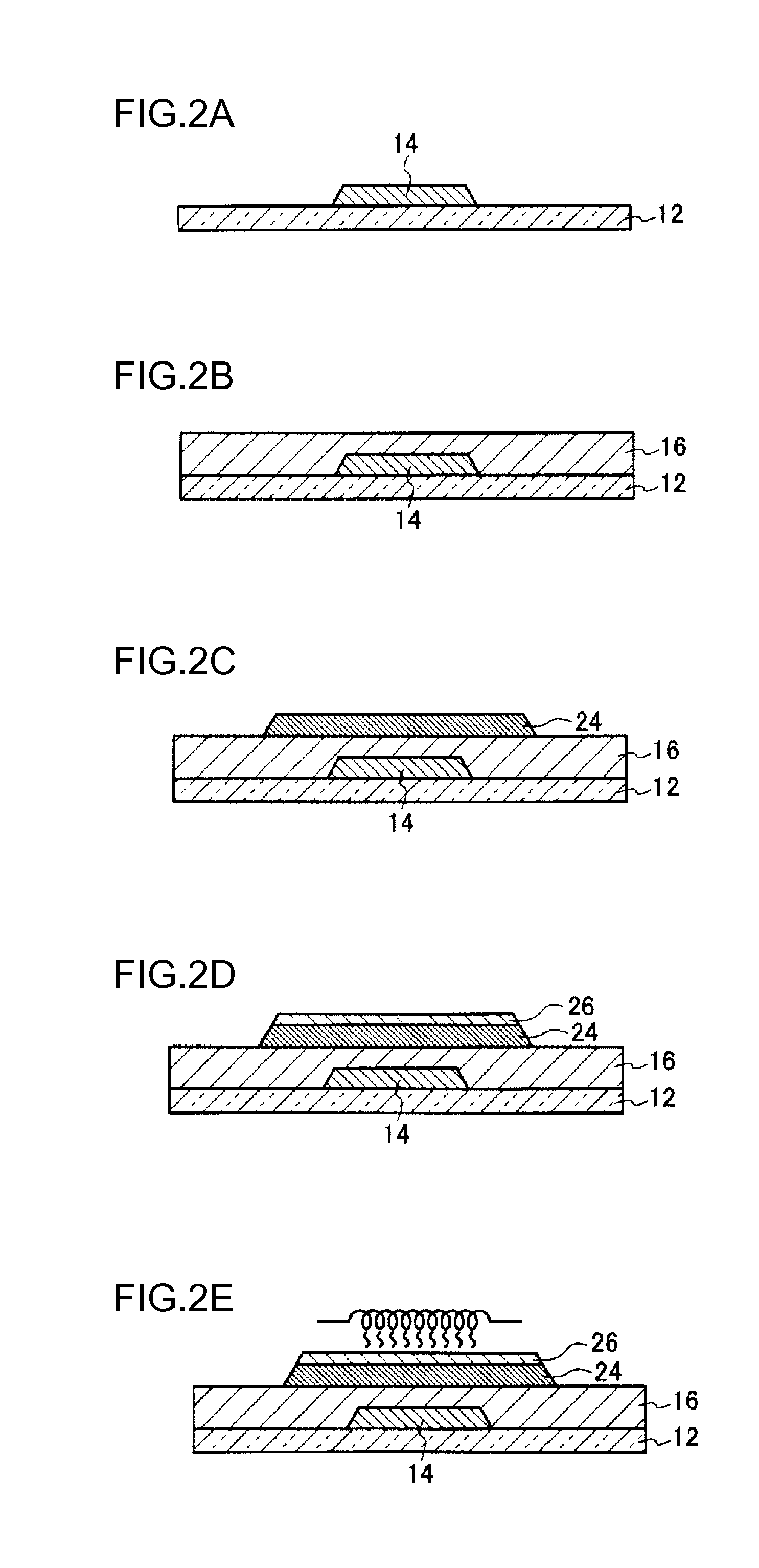
[0192]The TFT relating to Example 2 used the same fabrication method as TFT 500 apart from the heat treatment atmospheres in the heat treatment steps, meaning the third step and the fifth step. Specifically, in the third step, atmospheric air was used as the heat treatment atmosphere, and in the fifth step, an oxidizing atmosphere with an oxygen partial pressure of 100% was used as the heat treatment atmosphere. Thus, the TFT relating to Example 2 was obtained.
example 3
[0193]The TFT relating to Example 3 used the same fabrication method as TFT 500 apart from the heat treatment atmospheres in the heat treatment steps, the third step and the fifth step. Specifically, in the third step, an oxidizing atmosphere with an oxygen partial pressure of 100% was used as the heat treatment atmosphere, and in the fifth step, an oxidizing atmosphere with an oxygen partial pressure of 100% was used as the heat treatment atmosphere. Thus, the TFT relating to Example 3 was obtained.
experimental examples 1 to 4
[0206]For Experimental Example 1, a p-type silicon substrate with a thermal oxide film to serve as a gate electrode was prepared to be the substrate (1-inch square×1 mm thick; thickness t, 525 μm; thermal oxide film (silicon dioxide) thickness, 100 nm).
[0207]In concrete terms, the p-type silicon substrate with the thermal oxide film was prepared by resist application and baking, removal of silicon dioxide at the rear face by etching (using BHF), pure water washing, resist removal (using sulfuric acid / hydrogen peroxide), pure water washing and rinsing, and nitrogen blowing. Due to boron doping, the silicon substrate had a resistivity of 0.001 to 0.0013 Ωcm.
[0208]An IGZO film (In:Ga:Zn=1:1:1) was formed by DC sputtering to a thickness of 50 nm, under the following conditions: back pressure, 5×10⁻⁶ Pa; film formation pressure, 0.8 Pa; argon, 30 sccm (5.07×10⁻² Pa·m3 / s); oxygen (O2), 0.25 sccm (4.225×10⁻⁴ Pa·m3 / s); DC 50 W. Ordinarily, after the IGZO film is formed, patterning would be ...
PUM
 Abstract
Description
Claims
Application Information


