Device comprising an organic light emitting display

a technology of light-emitting displays and devices, which is applied in the manufacture of electrode systems, electric discharge tubes/lamps, discharge tubes luminescnet screens, etc., can solve the problems of poor adhesion properties of glass, low lifetime, and prone to breakag

Active Publication Date: 2015-02-24
SAMSUNG DISPLAY CO LTD +1
View PDF24 Cites 4 Cited by
  • Summary
  • Abstract
  • Description
  • Claims
  • Application Information

AI Technical Summary

Benefits of technology

[0010]By providing a bonding layer between the glass material and the layer comprising an organic polymeric material an structure is formed, which is less fragile, but still flexible. Furthermore, the bonding layer ensures that the sandwich structure remains durable and resists delamination.

Problems solved by technology

However, one problem is the sensitivity of the OLED materials to oxygen and / or moisture resulting in rather low lifetimes. This may e.g. be handled by placing the actual OLED components between two glass layers, which are essentially free of oxygen and / or vapor diffusion.
But such thin glass layers, i.e. below 50 μm, or even below 20 μm, have the problem that they become very fragile and tend to break due to their brittleness.
OLEDs with the above-mentioned structures, however, have the further problem that glass is a material which exhibits rather poor adhesion properties.
For example bonding of such a glass armed OLED display to a polymeric substrate or lamination thereof within a stack of polymeric layers leads to poor bonding durability.
In particular in case of lamination, delamination readily takes place, which is of particular disadvantage, if the OLED display is integrated into e.g. a value and / or security document, since separation of components of such documents may be utilized for making counterfeits by integration of obtained authentic components into such counterfeits.

Method used


Image

  • Device comprising an organic light emitting display
  • Device comprising an organic light emitting display

Examples


Embodiment Construction

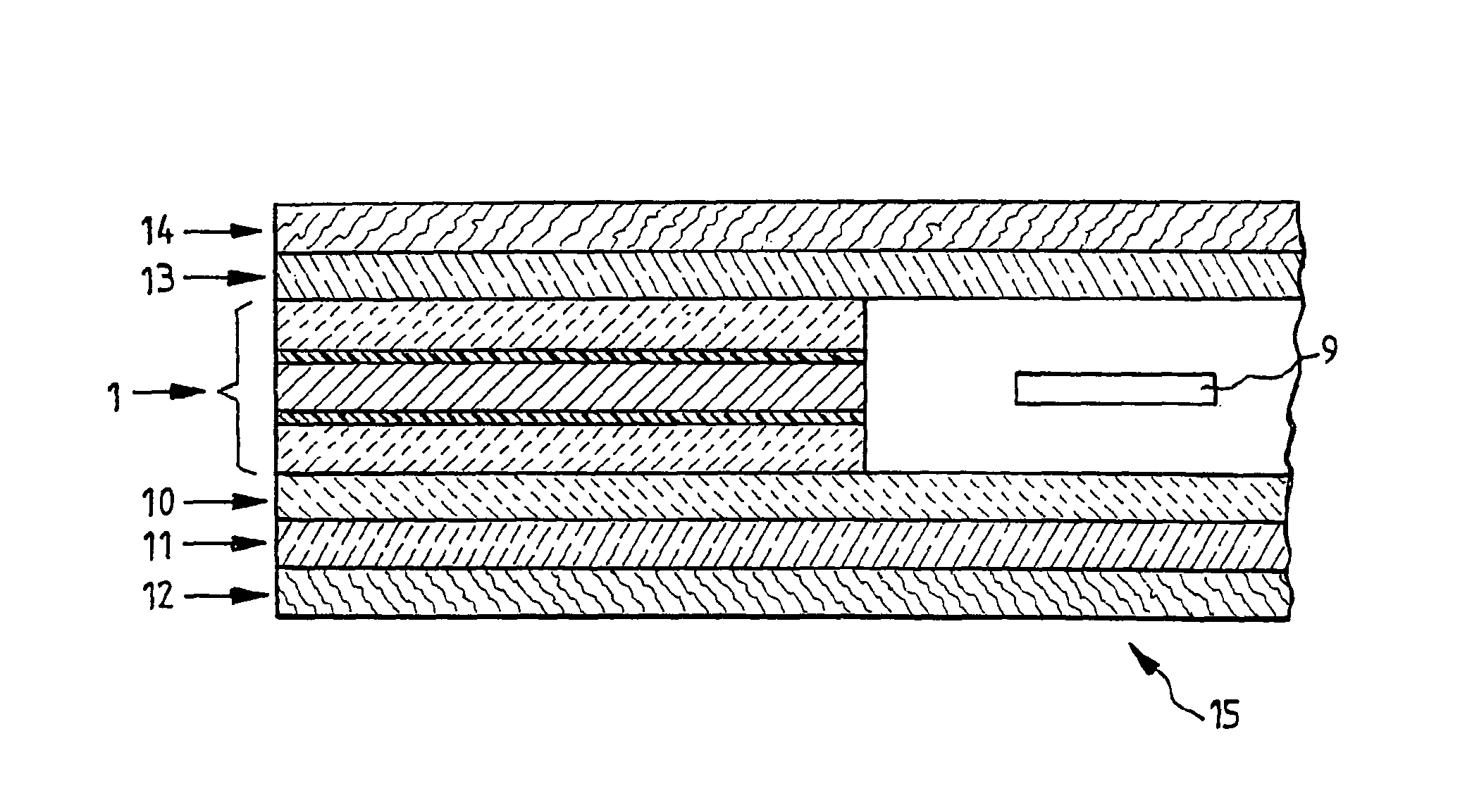
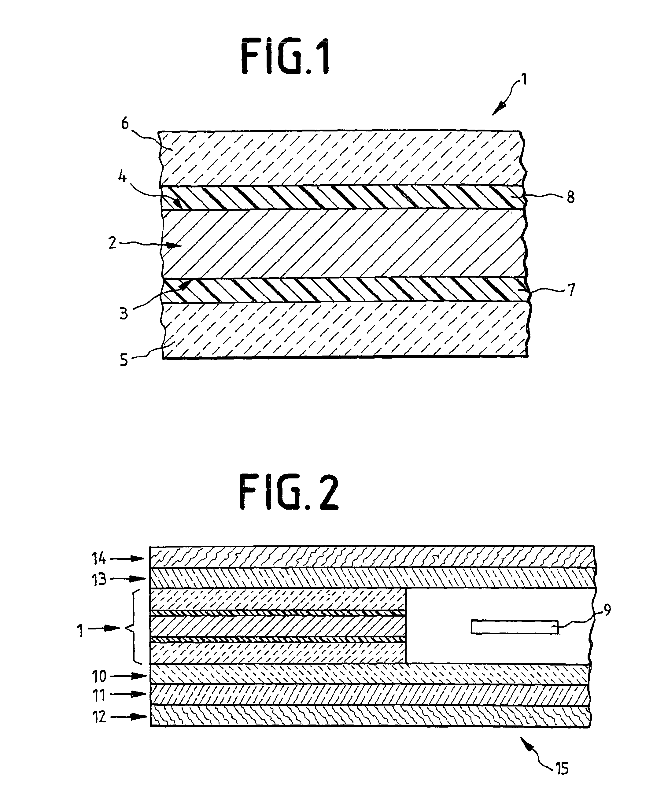
[0006]For achieving these objects, the invention teaches a sandwich structure comprising: an Organic Light Emitting Diode (OLED), wherein at least one of the both outer opposite surfaces of said OLED consists of a glass material, and at least one layer provided on the at least one outer opposite surface of said OLED consisting of glass, wherein said layer comprises an organic polymer material, and wherein said layer comprising an organic polymer material and said outer surface consisting of glass are bonded to each other in a stacking manner by an intermediate bonding layer.

[0007]The phrase OLED in this context includes displays which comprise a matrix of OLEDs and related drive circuits.

[0008]Within certain embodiments, both outer opposite surfaces of said OLED consist of glass. In other embodiments only one of the opposite surfaces consists of glass and the other one of a diffusion barrier layer material common in the OLED art. Such diffusion barrier materials comprise inorganic m...


PUM

PropertyMeasurementUnit
thicknessaaaaaaaaaa
thicknessaaaaaaaaaa
thicknessaaaaaaaaaa

Abstract

The invention relates to a sandwich structure (1) comprising a flexible Organic Light Emitting Diode (OLED) (2), wherein the opposite outer surfaces (3, 4) of said OLED (2) consist of a glass material, and at least one layer (5, 6) provided on at least one of said outer surfaces (3, 4) of said OLED (2) and comprising an organic polymer material, wherein said layer (5, 6) comprising an organic polymer material and said outer surface (3, 4) consisting of glass are bonded to each other in a stacking manner by a bonding layer (7, 8).

Description

FIELD OF THE INVENTION[0001]The invention relates to sandwich structures comprising Organic Light Emitting Displays (OLED), wherein the opposite outer surfaces of said OLED consist of a sealing or barrier layer e.g. consisting of a glass material. The invention further relates to devices comprising such sandwich structures and processes for manufacturing such sandwich structures and devices.BACKGROUND OF THE INVENTION[0002]OLEDs and displays comprising OLEDs have become increasingly interesting for display purposes, in particular for small devices, like hand held devices, including value and security documents, because they may be produced as very thin layers. Additionally, OLED displays may be flexible (sometimes called FOLEDs for Flexible Organic Light Emitting Diode) due to the fact that they can be made from films of organic materials on flexible substrates, including flexible drive circuits, thus being capable to be adapted to non-plane surfaces and / or incorporated into structu...

Claims


Application Information

Patent Timeline
Patent Type & Authority Patents(United States)
IPC IPC(8): H01J1/63H01J9/20H01J9/00B32B17/10B32B27/06B42D25/00B42D25/45C09K11/06H01L51/52H05B33/10
CPCB32B17/10073B32B17/1077B32B27/06H01L51/5237C09K11/06H05B33/10B42D2033/44B42D2033/46C09K2211/14B42D25/00B42D25/45H10K50/8445H10K50/841H10K59/10H10K85/10H10K50/11H10K50/84B42D25/465
Inventor FISCHER, JORGMUTH, OLIVERPAESCHKE, MANFREDHAGEMANN, MICHAELKIM, SUNGCHULLEE, JOHNHYUKHAN, DONGWONKWACK, JINHOLEE, JAEHOKANG, DONGHUNSHIN, DAEBEOMKIM, HYOJIN
Owner SAMSUNG DISPLAY CO LTD
Why Eureka
Try Eureka