Metamorphic long wavelength high-speed photodiode

a photodiode, long-wavelength technology, applied in the direction of semiconductor/solid-state device manufacturing, semiconductor devices, electrical apparatus, etc., can solve the problems of inability to meet the requirements of high-speed photodiodes. , the device is relatively expensive, the inp substrate is expensive and not available,

Inactive Publication Date: 2006-03-07
II VI DELAWARE INC
View PDF18 Cites 4 Cited by
  • Summary
  • Abstract
  • Description
  • Claims
  • Application Information

AI Technical Summary

Benefits of technology

[0016]The following summary of the invention is provided to facilitate an understanding of some of the innovative features unique to the present invention and is not intended to be a full description. A full appreciation of the various aspects of the invention can be gained by taking the entire specification, claims, drawings, and abstract as a whole.

Problems solved by technology

Unlike Silicon (Si) and Gallium Arsenide (GaAs), however, InP is not as well established and is very fragile.
In addition, InP substrates are expensive and not available in sizes as large as GaAs or Si.
Finally, gas phase epitaxial growth on InP requires the use of phosphine, which is often not available on particular epitaxial systems and causes several technical problems.
It is important to note, however, that despite materials compatibility and separate optimization control, such a device is relatively expensive, fragile, and difficult to process, requiring complicated integration into components.
That is, the growth run may be continuous and uninterrupted.
Based on the foregoing, those skilled in the art can appreciate that prior art manufacturing methods for semiconductor devices, such as photodiodes grown on InP substrates, are expensive, fragile, difficult to process, and additionally difficult to build into components.
Such processing complexity also results in inefficiencies and increased manufacturing expenses.

Method used


Image

  • Metamorphic long wavelength high-speed photodiode
  • Metamorphic long wavelength high-speed photodiode
  • Metamorphic long wavelength high-speed photodiode

Examples


Embodiment Construction

[0032]The particular values and configurations discussed in these non-limiting examples can be varied and are cited merely to illustrate an embodiment of the present invention and are not intended to limit the scope of the invention.

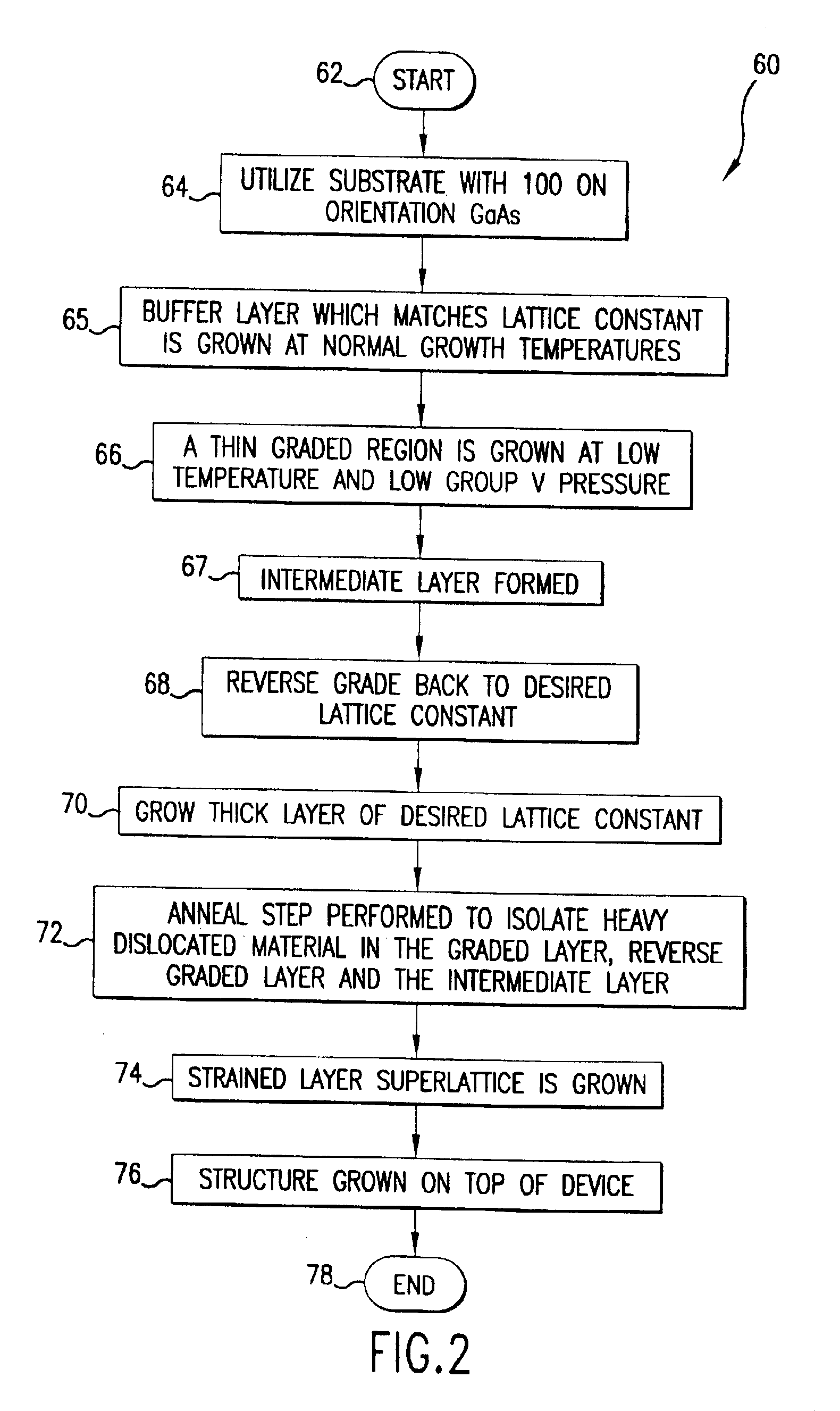
[0033]FIG. 2 is a flow chart illustrating operational steps for fabricating a semiconductor device in accordance with preferred embodiments of the present invention. A photodiode is one type of semiconductor device that can be fabricated according to the steps and processes disclosed herein. Thus, a photodiode device can be constructed according to the operations illustrated in FIG. 2. Using grading, an intermediate layer, an inverse grade, (100) nominally on orientation GaAs substrates, in-situ annealing, and a strained layer superlattice, artificial substrates can be created on which semiconductor devices, such as long-wavelength photodiodes, are fabricated.

[0034]The strained layer superlattice can be composed of a lower strain, a medium strain, and a ...


PUM


Abstract

A metamorphic device including a substrate structure upon which a semiconductor device can be formed. In the metamorphic device, a buffer layer matching a substrate lattice constant is formed at normal growth temperatures and a thin grading layer which grades past the desired lattice constant is configured at a low temperature. A reverse grading layer grades the lattice constant back to match a desired lattice constant. Thereafter, a thick layer is formed thereon, based on the desired lattice constant. Annealing can then occur to isolate dislocated material in at least the grading layer and the reverse grading layer. Thereon a strained layer superlattice is created upon which a high-speed photodiode or other semiconductor device can be formed.

Description

[0001]This application is a divisional application of application Ser. No. 09 / 766,797, filed on Jan. 22, 2001 now U.S. Pat. No. 6,558,973.BACKGROUND OF THE INVENTION[0002]The present invention relates to semiconductor devices and methods for manufacturing the same. The present invention also relates to photodiode devices and methods for manufacturing the same. The present invention additionally relates to high-speed, long-wavelength photodiode devices and improved methods for manufacturing the same. The present invention further relates to techniques for growing semiconductor photodiode devices on substrates.[0003]With the rapid development of lightwave communications, low-cost, high-performance optical photodiodes are required for a variety of system applications. Photodiodes are p-n junction semiconductor devices that produce a significant photocurrent when illuminated. Photodiodes operate based on principals of photoconductivity, which is an enhancement of the conductivity of p-n...

Claims


Application Information

Patent Timeline
Patent Type & Authority Patents(United States)
IPC IPC(8): H01L31/0336H01L31/0328H01L31/10H01L21/00H01L21/20H01L21/205H01L31/00H01L31/0304H01L31/18
CPCH01L21/02381H01L21/02395H01L21/02463H01L21/02505H01L21/02507H01L21/02546H01L31/105H01L31/184H01L21/0251Y10S438/938Y02E10/544
Inventor JOHNSON, RALPH H.GUENTER, JAMES K.BIARD, JAMES R.
Owner II VI DELAWARE INC
Why Eureka
Try Eureka