
Gate-all-around nanowire MOSFET and method of formation

a technology of nanowires and mosfets, which is applied in the field of gate-all-around nanowire mosfets and formation methods, complementary metal oxide semiconductor devices, etc., can solve the problems of increasing the parasitic capacitance of the mosfet, the bottom portion of the gate may become longer, and the difficulty (if not impossible) of patterning the portion of the gate located underneath the nanowir

Active Publication Date: 2015-03-03
GLOBALFOUNDRIES US INC
View PDF8 Cites 184 Cited by
  • Summary
  • Abstract
  • Description
  • Claims
  • Application Information

AI Technical Summary

Benefits of technology

This patent describes methods and apparatus for fabricating semiconductor devices using nanowires and dummy gates. The technical effects of this invention include reducing the size of transistors, improving performance, and increasing efficiency of semiconductor devices. Additionally, the invention allows for the formation of a gate-all-around structure in which the gate surrounds the nanowire, providing greater control and performance of the device.

Problems solved by technology

Formation of such a gate so as to wrap around the nanowire is a challenge.
For example, it is often difficult (if not impossible) to pattern the portion of the gate that is located underneath the nanowire.
Hence, the bottom portion of the gate may become longer than the top portion and may overlap the source and drain regions of the device.
However, the undercutting also extends the opening in the directions toward the source and drain, thereby adding to the parasitic capacitance of the MOSFET.

Method used


Image

  • Gate-all-around nanowire MOSFET and method of formation
  • Gate-all-around nanowire MOSFET and method of formation
  • Gate-all-around nanowire MOSFET and method of formation

Examples


Embodiment Construction

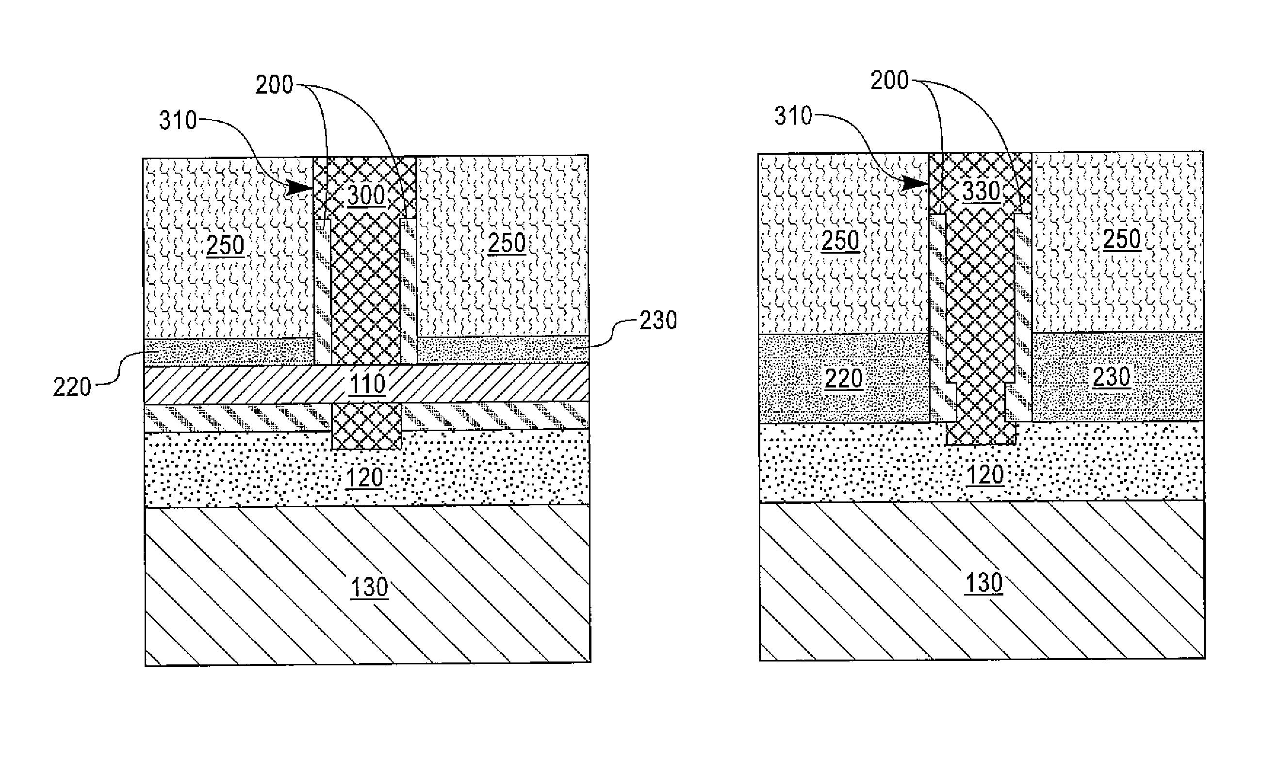
[0036]In the exemplary embodiments disclosed herein, GAA nanowire architecture is used in the fabrication of a CMOS such as a MOSFET to allow for improved electrostatic gate control in a conducting channel and to offer the potential to drive more current per device area than is possible in conventional planar CMOS architectures. In implementing the GAA nanowire architecture, a dummy gate comprising an oxide material is formed over a nanowire so as to extend substantially transverse to the nanowire. Lower portions of the dummy gate extend below and underneath the nanowire and into a surface on which the nanowire is disposed. Upper portions of the material of the dummy gate are removed, and lower portions of the material of the dummy gate (the oxide under the nanowire extending between source and drain regions) are recessed and undercut. Spacers are then formed on opposing sides of the dummy gate. When the oxide is undercut after removal of the upper portions of the dummy gate, the la...


PUM


Abstract

A method for fabricating a semiconductor device comprises forming a nanowire on an insulator layer at a surface of a substrate; forming a dummy gate over a portion of the nanowire and a portion of the insulator layer; forming recesses in the insulator layer on opposing sides of the dummy gate; forming spacers on opposing sides of the dummy gate; forming source regions and drain regions in the recesses in the insulator layer on opposing sides of the dummy gate; depositing an interlayer dielectric on the source regions and the drain regions; removing the dummy gate to form a trench; removing the insulator layer under the nanowire such that a width of the trench underneath the nanowire is equal to or less than a distance between the spacers; and forming a replacement gate in the trench.

Description

CROSS REFERENCE TO RELATED APPLICATION[0001]This application is a continuation of U.S. patent application Ser. No. 14 / 035,060, filed on Sep. 24, 2013, the contents of which are incorporated herein by reference in their entirety.BACKGROUND[0002]The exemplary embodiments of this invention relate generally to semiconductor devices and, more particularly, to a complementary metal oxide semiconductor device having a gate-all-around nanowire structure[0003]A complementary metal oxide semiconductor device (CMOS) uses symmetrically-oriented pairs of p-type and n-type metal oxide semiconductor field effect transistors (MOSFETs) arranged on silicon or silicon-on-insulator (SOI) substrates. Source and drain regions associated with each MOSFET are connected by a channel. A gate disposed adjacent the channel controls the flow of current between the source and drain regions. The channel may be defined by a thin “fin” or other structure that provides surface(s) through which the gate controls the ...

Claims


Application Information

Patent Timeline
Patent Type & Authority Patents(United States)
IPC IPC(8): H01L29/76H01L29/06H01L29/775H10K99/00
CPCH01L29/0669H01L29/775H01L29/66439H01L29/0847H01L29/78696H01L29/0673H01L29/66545H01L29/42392H01L21/82385H01L21/8238H01L29/4983H01L29/0676H10K85/221H01L29/495H01L29/4966H01L29/517H01L29/0649H01L29/1033H01L29/51H01L29/518H01L29/78603H01L29/78606
Inventor CHENG, KANGGUODORIS, BRUCE B.HASHEMI, POUYAKHAKIFIROOZ, ALIREZNICEK, ALEXANDER
Owner GLOBALFOUNDRIES US INC
Features
  • Generate Ideas
  • Intellectual Property
  • Life Sciences
  • Materials
  • Tech Scout
  • Unparalleled Data Quality
  • Higher Quality Content
  • 60% Fewer Hallucinations
Learn More