
Imaging apparatus

a technology of imaging apparatus and lens group, which is applied in the field of imaging apparatus, can solve the problems of insufficient consideration and insufficient consideration of imaging devices, and achieve the effects of reducing the thickness of the apparatus, reducing the overall optical length of the lens group, and reducing the cross-talk between adjacent pixels

Active Publication Date: 2015-03-24
FUJIFILM CORP
View PDF15 Cites 3 Cited by
  • Summary
  • Abstract
  • Description
  • Claims
  • Application Information

AI Technical Summary

Benefits of technology

The present invention provides an imaging apparatus with a solid-state image sensor that has a reduced thickness and downsized while maintaining favorable optical properties. Additionally, the imaging apparatus includes a color filter layer with separation walls to reduce cross-talk between pixels, and a pixel pitch and maximum incident angle that allow for a reduction in the overall optical length of the lens group and image sensor. The invention also reveals that incident angles up to 45 degrees are acceptable, providing high design flexibility.

Problems solved by technology

U.S. Patent Application Publication No. 20100245638 allows reduction in thickness of the image sensor but sufficient consideration is not given to the imaging device to which the image sensor is incorporated.
That is, sufficient consideration is not given to the relationship between the image sensor and imaging optical system in an imaging device, pixel pitch, light incident angle, and the like for realizing an imaging device having favorable optical properties with a reduced thickness.

Method used


Image

  • Imaging apparatus
  • Imaging apparatus
  • Imaging apparatus

Examples


Embodiment Construction

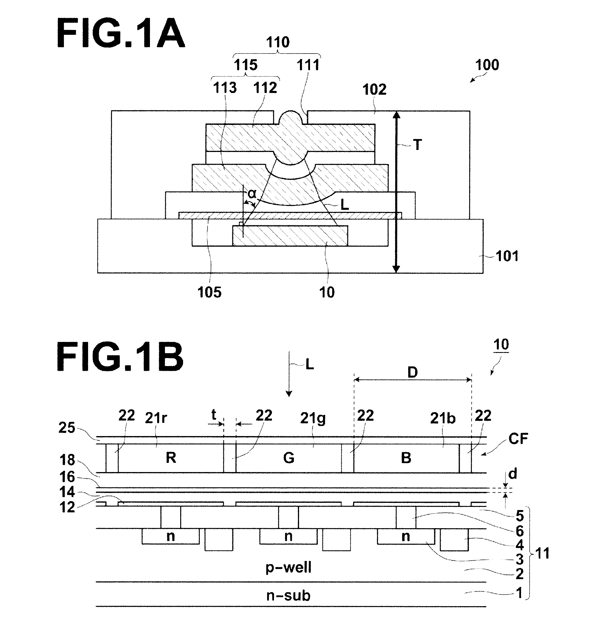
[0039]An imaging apparatus according to an embodiment of the present invention will now be described. FIG. 1A is a schematic cross-sectional view of an imaging apparatus according to an embodiment of the present invention, illustrating a structure thereof, and FIG. 1B is a schematic partial cross-sectional view of a solid-state image sensor provided in the imaging apparatus.

[0040]As illustrated in FIG. 1A, the imaging apparatus 100 includes a solid-state image sensor 10 incorporated in a ceramic package 101, and lenses 112, 113 fixedly disposed in a lens holder 102 having an aperture stop 111 so as to form an image on a surface (light receiving surface) of the solid-state image sensor 10, in which the ceramic package 101 and lens holder 102 are combined. An infrared light cut filter 105 is provided between a lens group of the lenses 112, 113 and solid-state image sensor 10. Here, an imaging optical system 110 is formed by the aperture stop 111 and lens group 115.

[0041]As illustrated...


PUM


Abstract

An imaging apparatus, including imaging optical system having a lens group and an aperture stop, and a solid-state image sensor which includes a photoelectric conversion layer made of an organic material and a color filter layer with color filters of two or more colors and a separation wall. The photoelectric conversion layer has a thickness of 0.1 82 m to 1 μm, each of the color filters has a refractive index of 1.5 to 1.8, the separation wall has a width of 0.05 μm to 0.2 μm and a refractive index of 1.22 to 1.34, and the lens group and the solid-state image sensor are disposed such that the relationship between a pixel pitch D (μm) of the sensor and a maximum angle α (°) of a principal ray incident on the sensor is 45≧α≧25.D−20 where D≦2.6 μm.

Description

TECHNICAL FIELD[0001]The present invention relates to an imaging apparatus having a solid-state image sensor made of a photoelectric conversion film of an organic material and a color filter stacked on top of each other.BACKGROUND ART[0002]As imaging devices, typified by digital cameras, can be downsized easily, they are built into various types of portable devices, such as cell phones, PDAs, and the like. Further, they are widely used as cameras of videophones or vehicle cameras for monitoring images of inside and outside of various types of vehicles from the driver seat. The imaging apparatus includes an imaging unit in which an imaging optical system and a solid-state image sensor that photoelectrically converts a subject image formed by the optical system are unitized, in addition to circuits for reading out an imaging signal by driving the solid-state image sensor and obtaining digitized image data by performing various types of signal processing on the imaging signal, and a me...

Claims


Application Information

Patent Timeline
Patent Type & Authority Patents(United States)
IPC IPC(8): H04N9/083H04N9/03H04N25/00G02B5/20G02B13/00H01L27/146
CPCH04N5/335G02B5/201G02B13/001H01L27/14621H01L27/14627H04N5/2257H01L27/14618H01L2924/0002H04N23/57H01L2924/00H01L27/146G02B3/00H04N23/00H04N25/00
Inventor ASANOTANI, TAKEHARU
Owner FUJIFILM CORP
Learn More