Method for manufacturing acoustic wave device
a manufacturing method and technology of acoustic waves, applied in piezoelectric/electrostrictive transducers, conductive pattern formation, transducer types, etc., can solve the problems of deterioration in line width processing accuracy, peeling of bonded surfaces, cracks in substrates, etc., to enhance tcf, excellent temperature coefficient of frequency, and increase rigidity of thermal spray films
- Summary
- Abstract
- Description
- Claims
- Application Information
AI Technical Summary
Benefits of technology
Problems solved by technology
Method used
Image
Examples
example 1
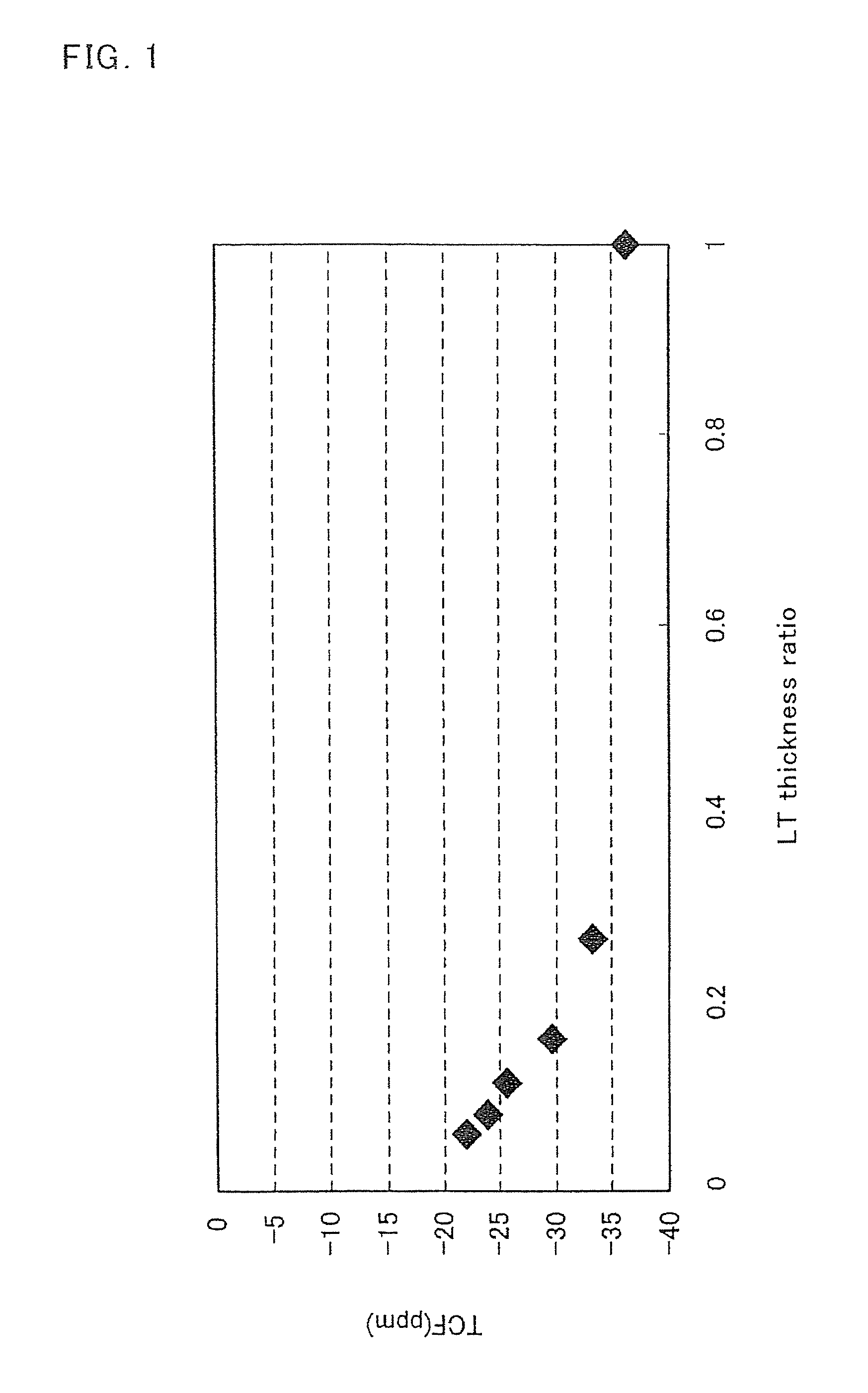
[0040]A substrate of lithium tantalate (LT substrate) was provided having a linear thermal expansion coefficient of 16×10−6 / K and a thickness of 0.02 mm, and mullite having a linear thermal expansion coefficient of 1×10⁻⁶ / K was thermal sprayed on one principal surface of the substrate at a thickness of 0.33 mm, thereby forming a 4-inch substrate. This 4-inch substrate was subjected to heating. Then, the 4-inch substrate was not cracked at heating temperatures of 180 and 200 degrees, however it was cracked at heating temperatures of 250 and 350 degrees.
[0041]Besides, instead of the LT substrate, a substrate of lithium niobate (LN substrate) having a linear thermal expansion coefficient of 15×10−6 / K and a thickness of 0.02 mm was used thereby to form a 4-inch substrate in the same way as mentioned above. This 4-inch substrate was subjected to heating. Then, the 4-inch substrate was not cracked at the heating temperatures of 180 and 200 degrees, however, it was cracked at the heating t...
example 2
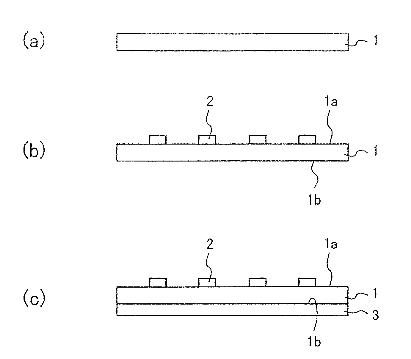
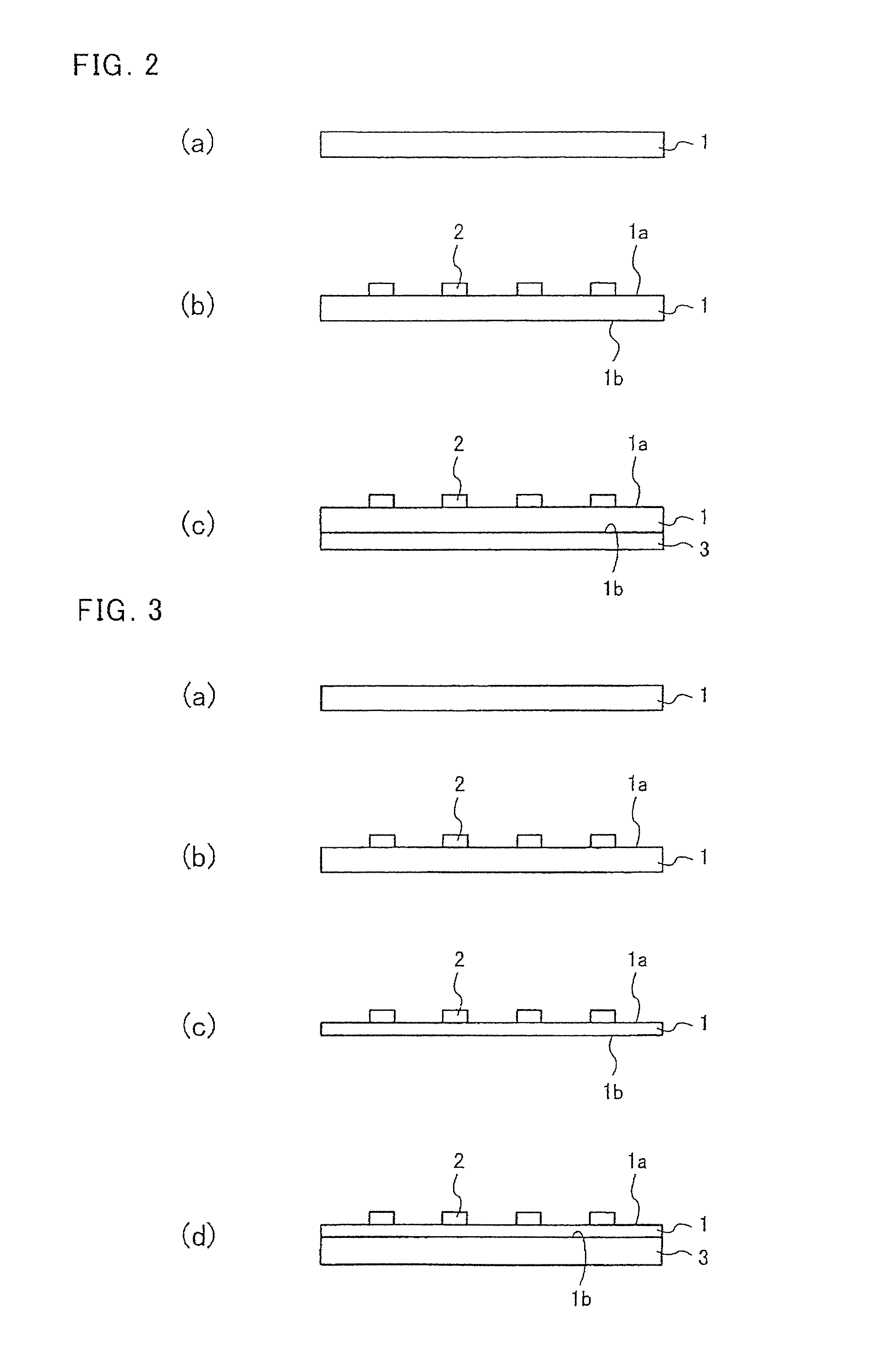
[0045]An IDT was formed on one principal surface of a substrate of lithium tantalate (LT substrate) having a linear thermal expansion coefficient of 16×10−6 / K, a diameter of 4 inches and a thickness of 0.25 mm. In this IDT forming, the resist used was a chemical amplification resist and the PEB (Post Exposure Bake) temperature was 110 degrees. Then, the opposite principal surface of the LT substrate was lapped to a thickness of 0.01 to 0.04 mm and roughened at Ra of 0.1 μm. Next, powders of silicon and alumina were thermal sprayed in this order on the roughened opposite principal surface so that a total thickness of the LT substrate and the thermal spray film was 0.25 mm. Here, the thermal spraying was performed with use of a DC plasma thermal spray device using Ar plasma gas and at power supply output of 40 kW.
[0046]The thus obtained wafer with IDT was examined as to the accuracy R of line width processing in the surface. This accuracy R was measured with an SEM (Scanning Electron ...
PUM
| Property | Measurement | Unit |
|---|---|---|
| Ra | aaaaa | aaaaa |
| surface roughness | aaaaa | aaaaa |
| roughness | aaaaa | aaaaa |
Abstract
Description
Claims
Application Information


