Method of healing defect at junction of semiconductor device using germanium

a technology of semiconductor devices and defects, applied in the direction of semiconductor devices, electrical equipment, basic electric elements, etc., can solve problems such as the probability of degradation

Active Publication Date: 2015-04-07
KOREA ADVANCED NANO FAB CENT +1
View PDF4 Cites 1 Cited by
  • Summary
  • Abstract
  • Description
  • Claims
  • Application Information

AI Technical Summary

Benefits of technology

[0013]Accordingly, the present invention has been made keeping in mind the above problems encountered in the related art, and an object of the present invention is to provide a method of healing defects at junctions of a semiconductor device using germanium, wherein annealing may be performed at 600˜700° C. for 1˜3 hr after formation of an n+ Ge region, so that defects at junctions of the semiconductor device may be healed.
[0014]Another object of the present invention is to provide a method of healing defects at junctions of a semiconductor device using germanium, wherein, in order to reduce the depth of junctions, germanide may be formed via annealing after formation of an electrode, thus minimizing leakage current.

Problems solved by technology

Conventional semiconductors essentially involve an ion doping process, and defects at junctions having different conductive types are obstacles to improving properties of fine semiconductor devices depending on increases in the speed and degree of integration of the devices.
However, such conventional techniques do not disclose any specific method for healing defects at junctions, and also most other techniques do not show any special interest therein.
Furthermore, techniques disclosed to heal defects do not specify the temperature ranges and vaguely describe them in terms of annealing at high temperature.
So, reliable methods able to heal defects have not yet been introduced.
Moreover, upon annealing at high temperature, there exists a probability of degradation because leakage current occurs due to deepened junctions.

Method used


Image

  • Method of healing defect at junction of semiconductor device using germanium
  • Method of healing defect at junction of semiconductor device using germanium
  • Method of healing defect at junction of semiconductor device using germanium

Examples


Embodiment Construction

[0027]The present invention addresses a method of healing defects at junctions of a semiconductor device, by performing annealing, in particular, annealing at 600˜700° C. for 1˜3 hr after formation of an n+ Ge region.

[0028]Hereinafter, a detailed description will be given of the present invention with reference to the appended drawings.

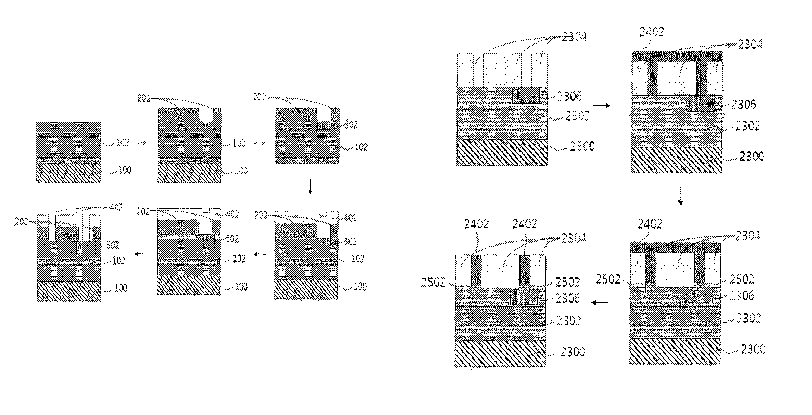
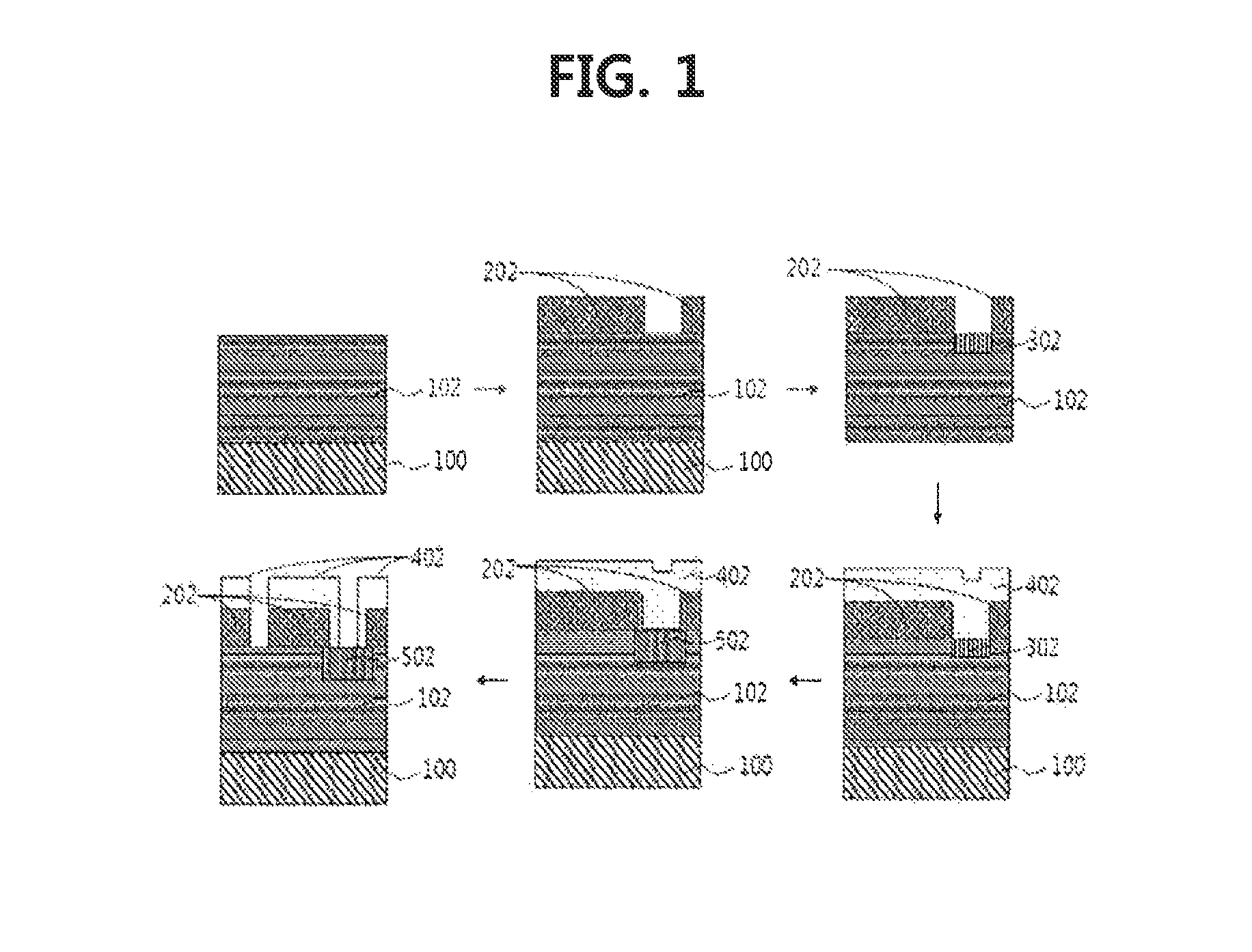
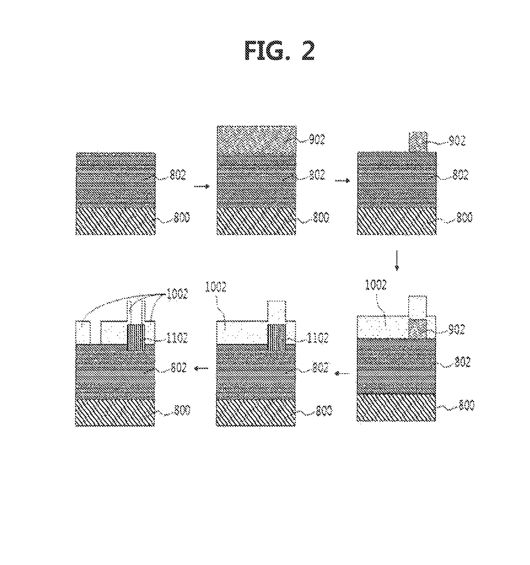
[0029]FIGS. 1, 2 and 3A and 3B schematically illustrate three kinds of processes according to the present invention, and FIGS. 4A to 4D schematically illustrate formation of an electrode using the above processes.

[0030]The present invention is embodied by three kinds of processes.

[0031]Specifically, as illustrated in FIGS. 1 and 4A, Process 1 includes: 1) growing a p-Ge layer 102 on a substrate 100; 2) depositing an oxide film 202 on the p-Ge layer 102 and patterning the oxide film, thus forming a pattern for an n+ Ge region 302; 3) subjecting the pattern for an n+ Ge region 302 to ion implantation using a n-type dopant, thus forming an n+ Ge region 3...


PUM


Abstract

This invention relates to a method of healing defects at junctions of a semiconductor device, which includes growing a p-Ge layer on a substrate, performing ion implantation on the p-Ge layer to form an n+ Ge region or performing in-situ doping on the p-Ge layer and then etching to form an n+ Ge region or depositing an oxide film on the p-Ge layer and performing patterning, etching and in-situ doping to form an n+ Ge layer, forming a capping oxide film, performing annealing at 600˜700° C. for 1˜3 hr, and depositing an electrode, and in which annealing enables Ge defects at n+ / p junctions to be healed and the depth of junctions to be comparatively reduced, thus minimizing leakage current, thereby improving properties of the semiconductor device and achieving high integration and fineness of the semiconductor device.

Description

CROSS-REFERENCE TO RELATED APPLICATION[0001]This application claims the benefit of Korean Patent Application No. 10-2012-0157977, filed Dec. 31, 2012, which is hereby incorporated by reference in its entirety into this application.BACKGROUND OF THE INVENTION[0002]1. Technical Field[0003]The present invention relates to a method of healing defects at junctions of a semiconductor device, and more particularly, to a method of healing defects at junctions of a semiconductor device using germanium (Ge), wherein annealing is performed at 600˜700° C. for 1˜3 hr after formation of an n+ Ge region, thus healing defects at junctions of the semiconductor device.[0004]2. Description of the Related Art[0005]Field effect transistors using a silicon substrate control drain current via changes in the channel region depending on the magnitude of voltage applied to a gate, and are manufactured by defining an oxide film or a photoresist using photolithography to form a p-type well and an n-type source...

Claims


Application Information

Patent Timeline
Patent Type & Authority Patents(United States)
IPC IPC(8): H01L21/265H01L21/322
CPCH01L21/3221H01L21/26513H01L21/28512H01L21/324H01L29/45H01L21/28518H01L21/26
Inventor PARK, WON KYUHEO, JONG GONJUN, DONG HWANPARK, JIN HONGSHIM, JAE WOO
Owner KOREA ADVANCED NANO FAB CENT
Why Eureka
Try Eureka