Light absorption and filtering properties of vertically oriented semiconductor nano wires

a technology of vertical orientation and filtering properties, applied in the direction of optical filters, spectral modifiers, optical radiation measurement, etc., can solve the problems of inability to easily and accurately position nanostructures in functional devices, less robustness

Inactive Publication Date: 2015-04-07
PRESIDENT & FELLOWS OF HARVARD COLLEGE +1
View PDF474 Cites 240 Cited by
  • Summary
  • Abstract
  • Description
  • Claims
  • Application Information

AI Technical Summary

Problems solved by technology

However, these conventional approaches often require complex chemical synthesis or post-synthesis manipulation, and thus are less robust against minute variations of conditions and cannot easily and accurately position nanostructures in a functional device.

Method used


Image

  • Light absorption and filtering properties of vertically oriented semiconductor nano wires
  • Light absorption and filtering properties of vertically oriented semiconductor nano wires
  • Light absorption and filtering properties of vertically oriented semiconductor nano wires

Examples


examples

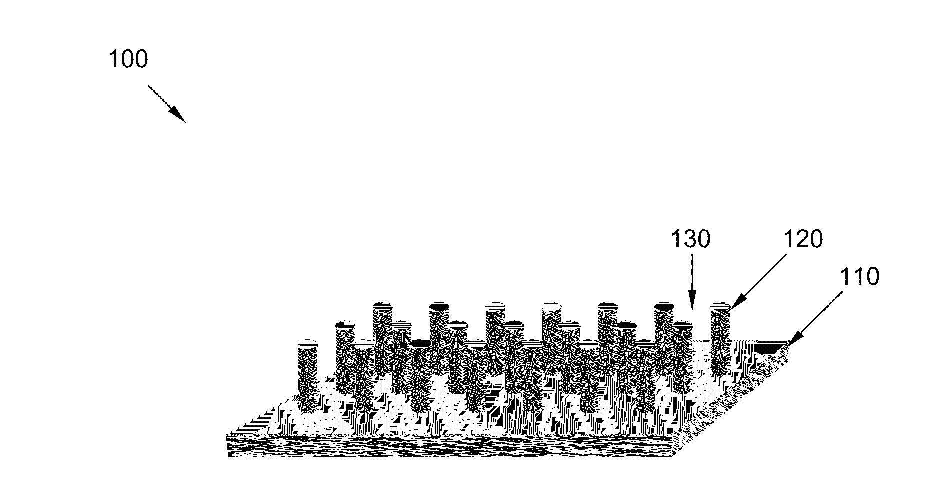
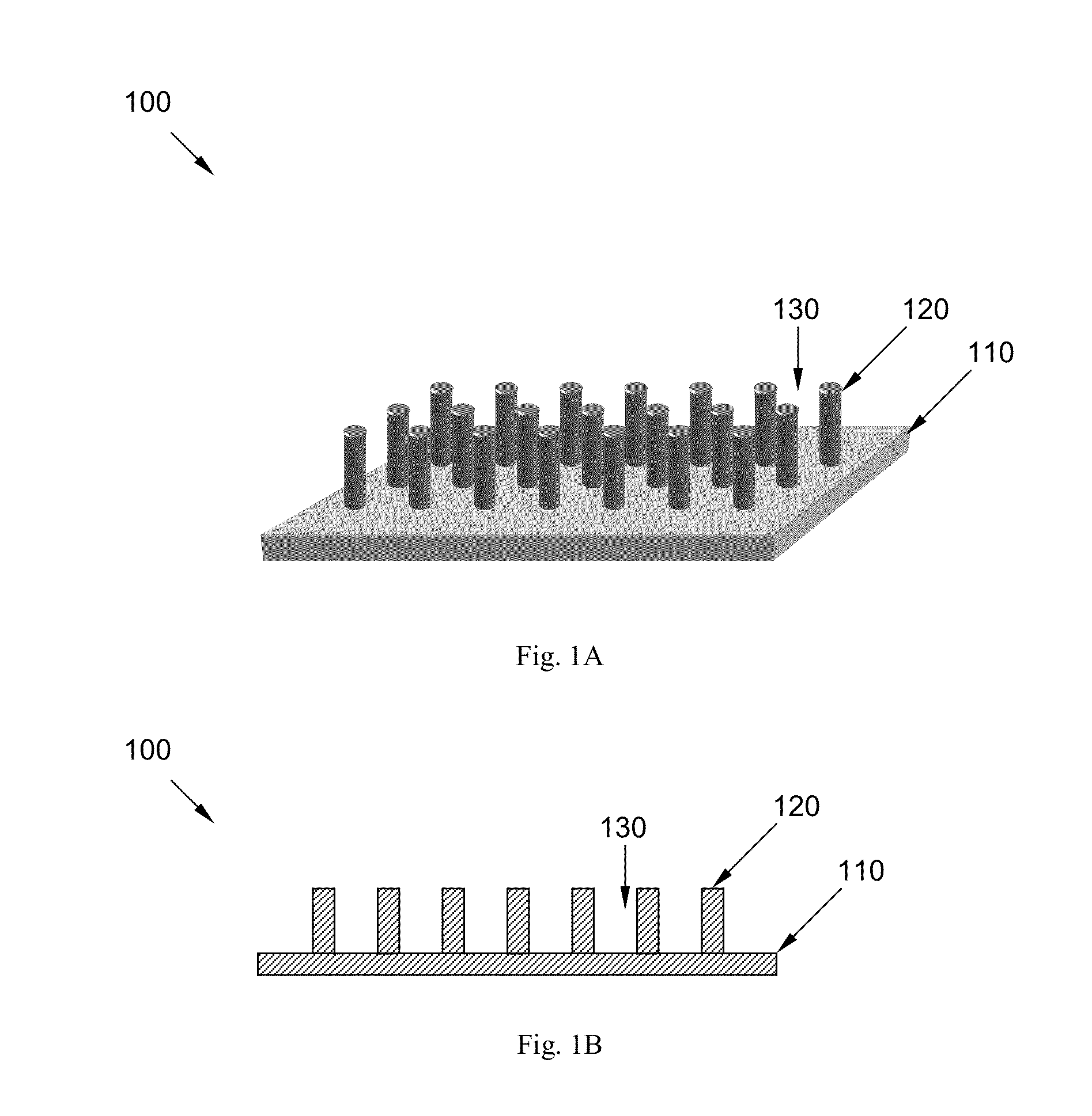
[0046]FIGS. 1A and 1B show schematics of a nanowire array 100, according to an embodiment. The nanowire array 100 comprises a substrate 110 and a plurality of nanowires 120 extending essentially vertically from the substrate 110 (e.g. angles between the nanowires 120 and the substrate 110 are from 85° to 90°). Each nanowire 120 preferably has uniform chemical composition along its entire length. Each nanowire 120 is single crystalline, multi-crystalline or amorphous. The nanowires 120 preferably are made of a suitable semiconductor or an electrically insulating materials, examples of which include Si, Ge, GaN, GaAs, SiO2, Si3N4, etc. A ratio of the refractive index (i.e., refractive index contrast) of the nanowires 120 and the refractive index of a cladding 130 (i.e., materials surround the nanowires 120) is preferably at least 2, more preferably at least 3. Radii of the nanowires 120 preferably are from 10 to 1000 nm, more preferably from 20 to 80 nm, most preferably from 45 to 75 ...


PUM

PropertyMeasurementUnit
radiiaaaaaaaaaa
distanceaaaaaaaaaa
diameteraaaaaaaaaa

Abstract

A nanowire array is described herein. The nanowire array comprises a substrate and a plurality of nanowires extending essentially vertically from the substrate; wherein: each of the nanowires has uniform chemical along its entire length; a refractive index of the nanowires is at least two times of a refractive index of a cladding of the nanowires. This nanowire array is useful as a photodetector, a submicron color filter, a static color display or a dynamic color display.

Description

CROSS-REFERENCE TO RELATED APPLICATIONS[0001]This application is related to U.S. patent application Ser. No. 12 / 204,686 (granted as U.S. Pat. No. 7,646,943), Ser. Nos. 12 / 648,942, 12 / 270,233, 12 / 472,264, 12 / 472,271, 12 / 478,598, 12 / 573,582, 12 / 575,221, 12 / 633,323, 12 / 633,318, 12 / 633,313, 12 / 633,305, 12 / 621,497, 12 / 633,297, 61 / 266,064, 61 / 357,429, 61 / 306,421, and 61 / 306,421, the disclosures of which are hereby incorporated by reference in their entirety.BACKGROUND OF THE INVENTION[0002]Nanostructures often exhibit fascinating physical properties not present in their bulk counterparts. Optical properties of nanostructures have been one of the recent research focuses. Tuning optical properties of nanostructures would facilitate their applications in the semiconductor, optics, and consumer electronics industry. In one example, optical properties of nanostructures can be controlled by their chemical composition. Chemical doping can change electronic structures of the materials semiconduct...

Claims


Application Information

Patent Timeline
Patent Type & Authority Patents(United States)
IPC IPC(8): G01J1/42B82Y20/00B82Y30/00B82Y40/00H01L27/146H01L31/0352
CPCB82Y30/00B82Y20/00B82Y40/00H01L27/14629H01L31/035227G02B5/22H01L27/1446H01L31/18Y10S977/762Y10S977/888Y10S977/954Y10T428/24174Y10T428/24893B82B1/00G02B5/20B82Y99/00F21V9/08G09F13/00H01L27/14603H01L27/14607H01L27/14692H01L31/107
Inventor SEO, KWANYONGWOBER, MUNIBSTEINVURZEL, PAULSCHONBRUN, ETHANDAN, YAPINGCROZIER, KENNETH B.
Owner PRESIDENT & FELLOWS OF HARVARD COLLEGE
Why Eureka
Try Eureka