Semiconductor device

a technology of semiconductor devices and semiconductors, applied in semiconductor devices, semiconductor/solid-state device details, electrical apparatus, etc., can solve the problems of excessive current density and decrease of withstanding voltage of semiconductor devices, and achieve the effects of reducing short-circuit energy density, reducing temperature increase of semiconductor devices, and improving short-circuit capacity

Inactive Publication Date: 2015-04-14
DENSO CORP
View PDF9 Cites 1 Cited by
  • Summary
  • Abstract
  • Description
  • Claims
  • Application Information

AI Technical Summary

Benefits of technology

[0008]The present invention provides a technique that is able to improve a short circuit capacity and to restrain a decrease of a withstanding voltage of a semiconductor device.
[0011]In the semiconductor device, the effective carrier amount of the channel parts is large in the first region (a region covered with the heat dissipation member) and is small in the second region (a region not covered with the heat dissipation member). This makes it possible to decrease a short-circuit energy density in the second region not covered by a heat dissipation member, at the time when the semiconductor device causes short-circuit. Furthermore, the heat dissipation member is disposed above the first region while the short-circuit energy density in the first region is large. This makes it possible to suitably restrain a temperature increase of the semiconductor device, thereby making it possible to improve a short circuit capacity. Further, since the first region and the second region have the same density of the trench gate electrodes, it is possible to restrain an electric field from concentrating on tips of the trench gate electrodes. This accordingly makes it possible to restrain a decrease of a withstanding voltage of the semiconductor device. Further, in the semiconductor device, the first semiconductor layer (a part where the channel parts are formed) and the second semiconductor layer (a part where no channel part is formed) are disposed in positions opposite to the trench gate electrodes. Hereby, the first semiconductor layer and the second semiconductor layer are placed appropriately, and thus, it is possible to flow a current through the entire of the first region and the second region generally uniformly.

Problems solved by technology

This easily causes electric field concentration in tips of the trench gate electrodes in the outer peripheral part, which may decrease a withstanding voltage of the semiconductor device.
However, in such a technique, a current flows only to part (a trench gate electrode where an emitter region is formed) of the outer peripheral part, which may cause a current density thereof to be excessive.

Method used


Image

  • Semiconductor device
  • Semiconductor device
  • Semiconductor device

Examples


Embodiment Construction

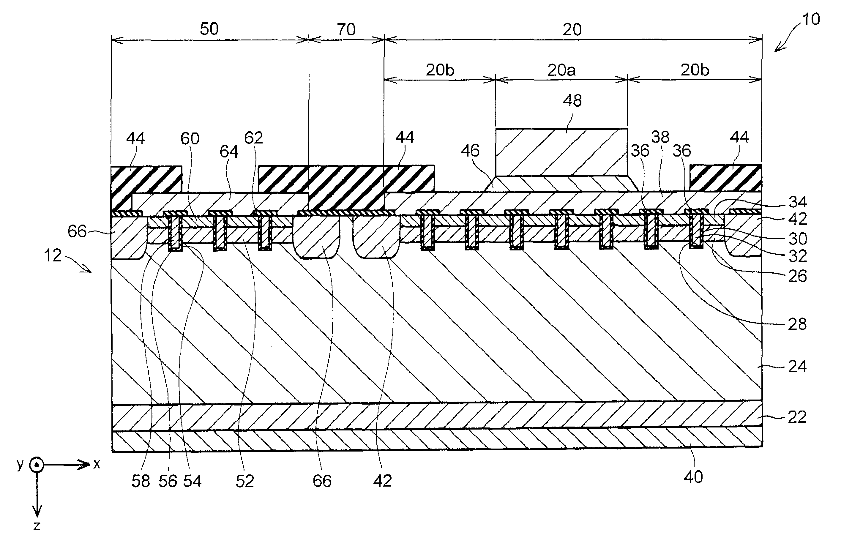
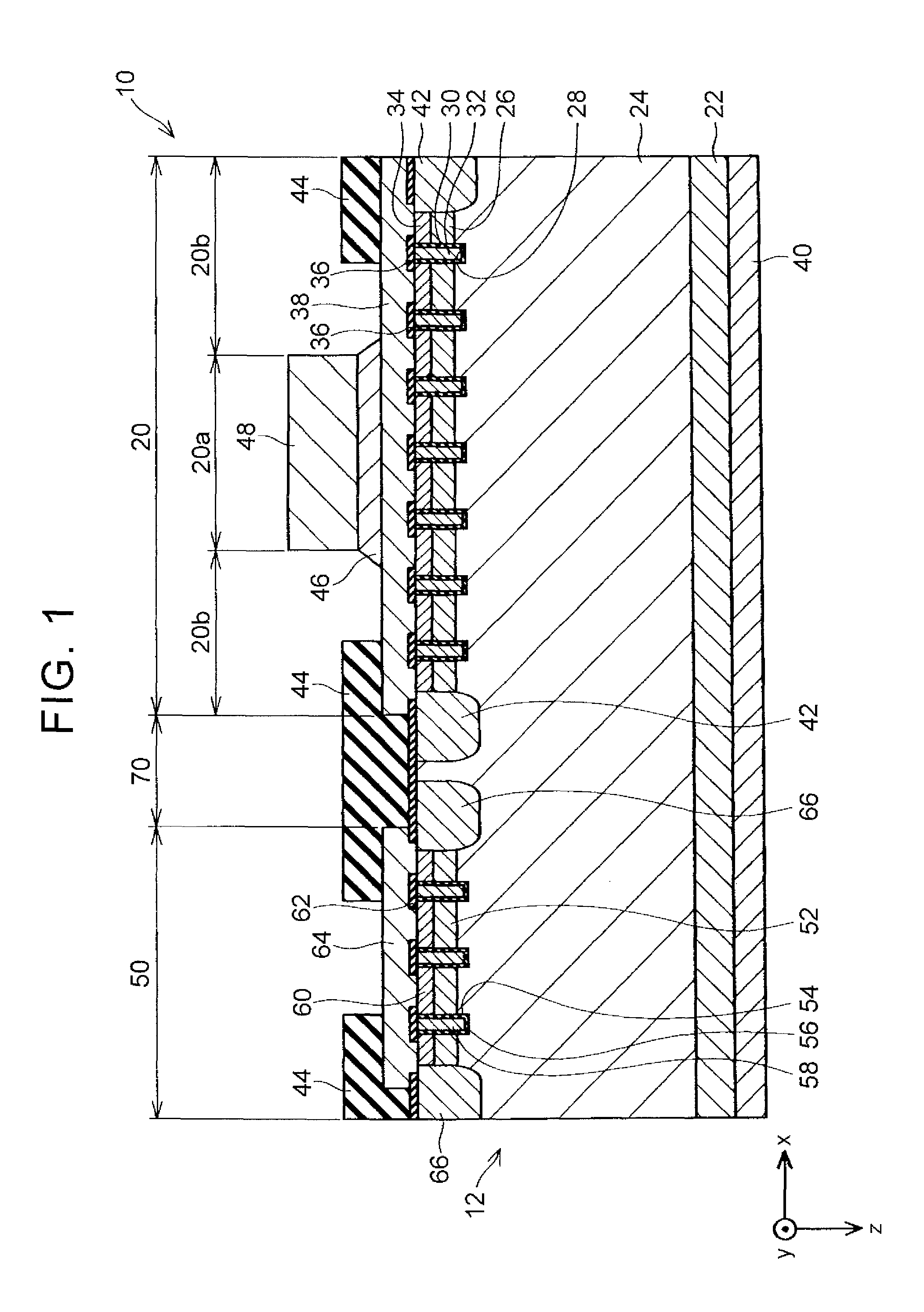
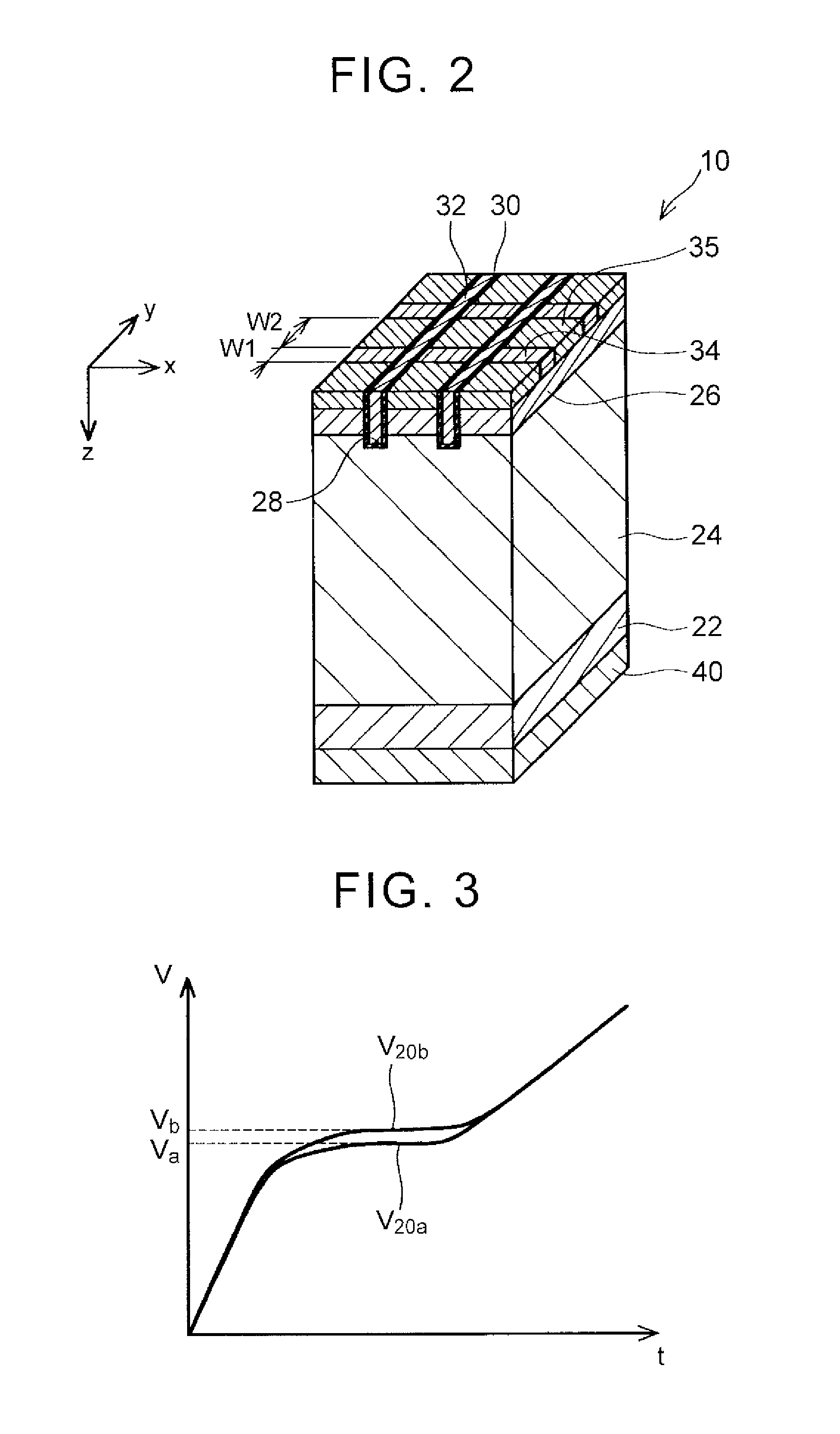
[0018]In a semiconductor device described in the present specification, a first-conductivity impurity concentration of a first semiconductor layer in a first region may be equal to a first-conductivity impurity concentration of a first semiconductor layer in a second region. When the semiconductor substrate is viewed in a plane manner, a value obtained by dividing an area of channel parts formed in the first region by an area of the first region may be larger than a value obtained by dividing an area of channel parts formed in the second region by an area of the second region. According to such a configuration, without causing the impurity concentration of the first semiconductor layer in the first region to differ from that in the second region, it is possible to lower a short-circuit energy density of the second region than a short-circuit energy density of the first region. Accordingly, it is possible to form the first semiconductor layer of the first region and the first semicon...


PUM


Abstract

In a semiconductor substrate of a semiconductor device, a drift layer, a body layer, an emitter layer, and a trench gate electrode are formed. When the semiconductor substrate is viewed in a plane manner, the semiconductor substrate is divided into a first region covered with a heat dissipation member, and a second region not covered with the heat dissipation member. A density of trench gate electrodes in the first region is equal to a density of trench gate electrodes in the second region. A value obtained by dividing an effective carrier amount of channel parts formed in the first region by an area of the first region is larger than a value obtained by dividing an effective carrier amount of channel parts formed in the second region by an area of the second region.

Description

INCORPORATION BY REFERENCE[0001]The disclosure of Japanese Patent Application No. 2013-109360 filed on May 23, 2013 including the specification, drawings and abstract is incorporated herein by reference in its entirety.BACKGROUND OF THE INVENTION[0002]1. Field of the Invention[0003]A technique disclosed in the present specification relates to a semiconductor device including a heat dissipation member.[0004]2. Description of Related Art[0005]In order to improve a short circuit capacity of a semiconductor device, a semiconductor device including a heat dissipation member is developed (for example, Japanese Patent Application Publication No. 2007-110002 (JP 2007-110002 A)). In the semiconductor device in JP 2007-110002 A, an IGBT (Insulated Gate Bipolar Transistor) is formed in an element region of a semiconductor substrate. An emitter electrode is formed on a top surface of the semiconductor substrate, and a heat spreader (a heat dissipation member) is disposed on a top surface of the...

Claims


Application Information

Patent Timeline
Patent Type & Authority Patents(United States)
IPC IPC(8): H01L27/06H01L29/739
CPCH01L29/7395H01L23/3677H01L29/7397H01L29/063H01L2224/32245H01L2924/0002H01L2924/13055H01L2924/13091H01L2924/00
Inventor MISUMI, TADASHI
Owner DENSO CORP
Why Eureka
Try Eureka