Active memory data compression system and method

a data compression and active memory technology, applied in the field of memory devices, can solve the problems of essentially no more efficient active memory devices, limited data paths between discrete dram devices and processors, and limited processing speed of computer systems using active memory devices

Active Publication Date: 2015-04-21
MICRON TECH INC
View PDF27 Cites 378 Cited by
  • Summary
  • Abstract
  • Description
  • Claims
  • Application Information

AI Technical Summary

Problems solved by technology

In contrast, the data path between a discrete DRAM device and a processor is normally limited by constraints on the size of external data buses.
Although an active memory device allows much more efficient processing of data stored in memory, the processing speed of a computer system using active memory devices is somewhat limited by the time required to transfer operand data to the active memory for processing and the time required to transfer results data from the active memory after the operand data has been processed.
During such data transfer operations, active memory devices are essentially no more efficient than passive memory devices that also require data stored in the memory device to be transferred to and from an external device, such as a CPU.

Method used


Image

  • Active memory data compression system and method
  • Active memory data compression system and method
  • Active memory data compression system and method

Examples


Embodiment Construction

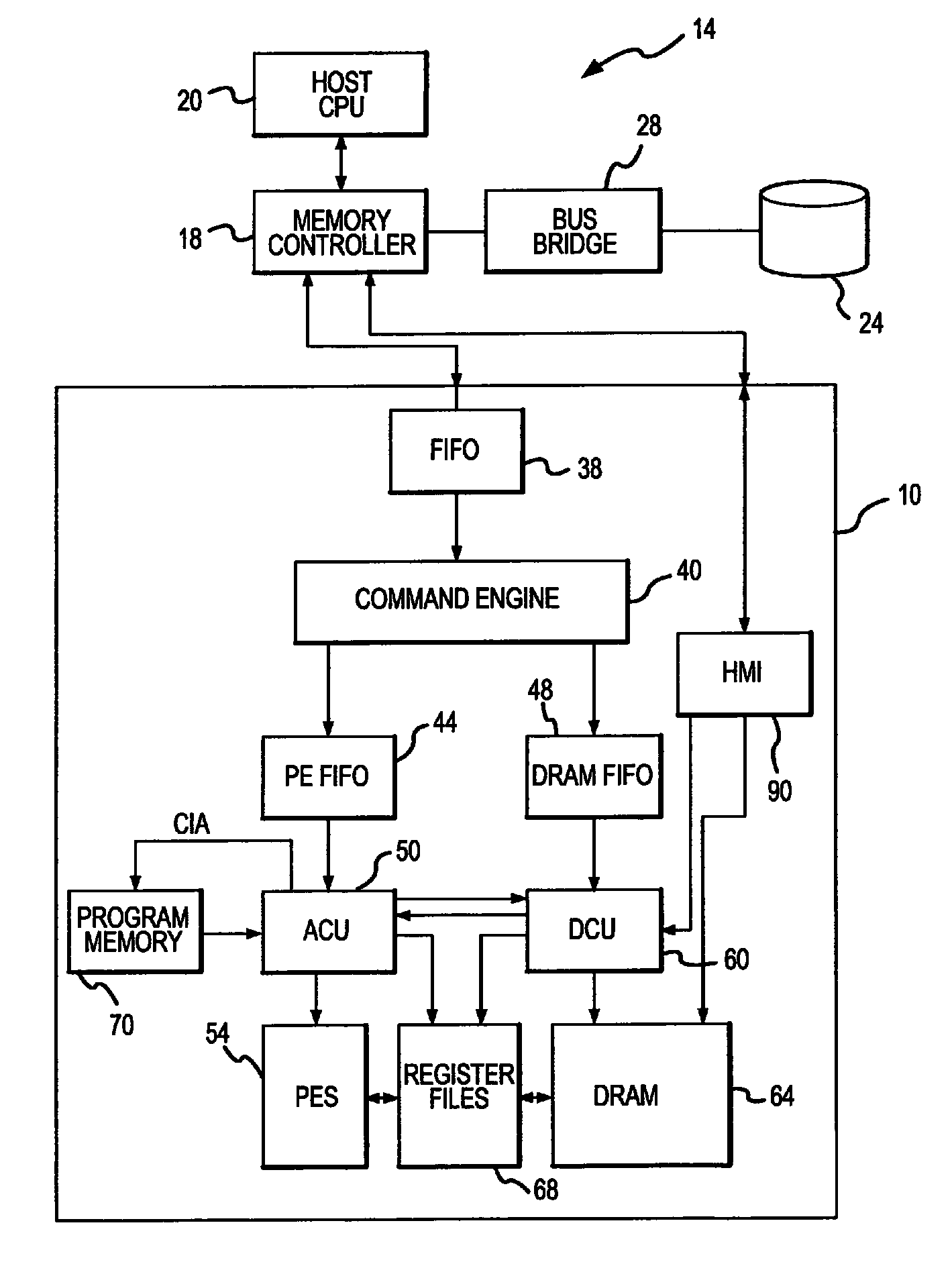
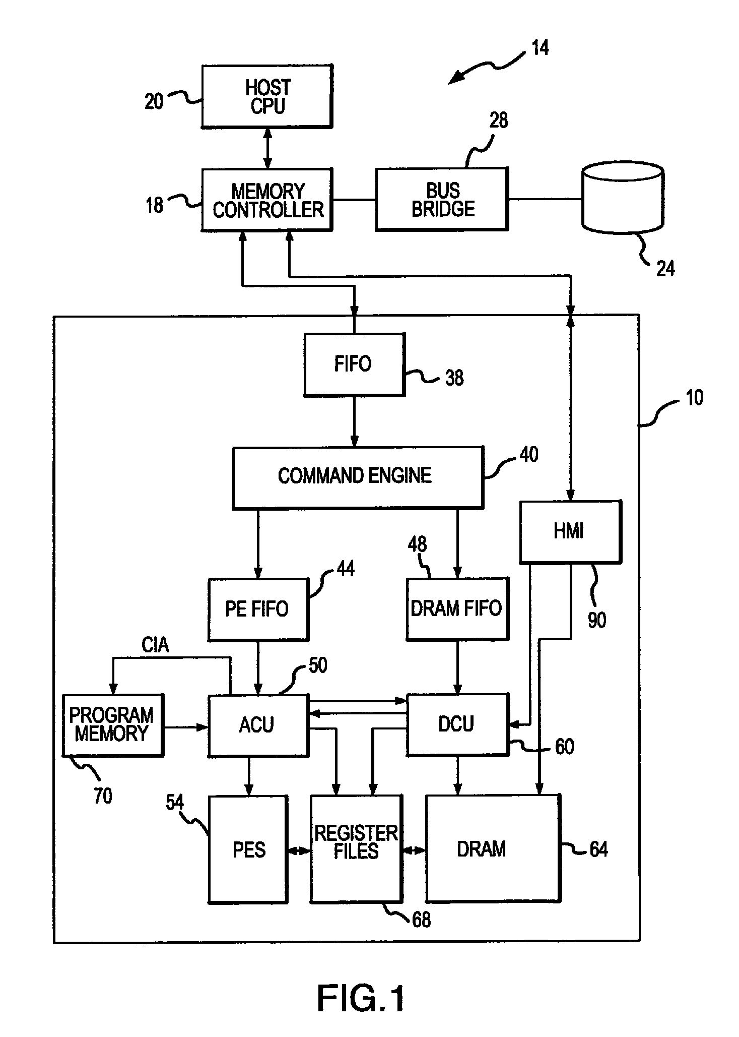
[0015]FIG. 1 shows an active memory device 10 according to one embodiment of the invention. The memory device 10 is preferably a component in a host system 14, which may include a memory controller 18, a host CPU 20, a mass storage device 24, such as a disk drive, a bus bridge 28 coupled between the memory controller 18 and the mass storage device 24, and other components that have been omitted from the host system 14 shown in FIG. 1 for the purpose of brevity and clarity. For example, a network (not shown), such as a local area network (“LAN”), may be coupled to the bus bridge 28. Also, a high speed interface (not shown), such as an Infiniband or Hypertransport interface, could be coupled to the memory controller 18. Other variations to the host system 14 shown in FIG. 1 will be apparent to one skilled in the art.

[0016]The active memory device 10 includes a first in, first out (“FIFO”) buffer 38 that receives high level task commands from the host system 14, which may also include ...


PUM


Abstract

An integrated circuit active memory device receives task commands from a component in a host computer system that may include the active memory device. The host system includes a memory controller coupling the active memory device to a host CPU and a mass storage device. The active memory device includes a command engine issuing instructions responsive to the task commands to either an array control unit or a DRAM control unit. The instructions provided to the DRAM control unit cause data to be written to or read from a DRAM and coupled to or from either the processing elements or a host / memory interface. The processing elements execute instructions provided by the array control unit to decompress data written to the DRAM through the host / memory interface and compress data read from the DRAM through the host / memory interface.

Description

TECHNICAL FIELD[0001]This invention relates memory devices, and, more particularly, to techniques for efficiently transferring data to and from active memory devices.BACKGROUND OF THE INVENTION[0002]A common computer processing task involves sequentially processing large numbers of data items, such as data corresponding to each of a large number of pixels in an array. Processing data in this manner normally requires fetching each item of data from a memory device, performing a mathematical or logical calculation on that data, and then returning the processed data to the memory device. Performing such processing tasks at high speed is greatly facilitated by a high data bandwidth between the processor and the memory devices. The data bandwidth between a processor and a memory device is proportional to the width of a data path between the processor and the memory device and the frequency at which the data are clocked between the processor and the memory device. Therefore, increasing ei...

Claims


Application Information

Patent Timeline
Patent Type & Authority Patents(United States)
IPC IPC(8): G06F13/14G06F9/30G06F12/00G06F9/38G06F13/12G06F15/78
CPCG06F9/3879G06F9/30036G06F9/3887G06F15/785G06F15/7821
Inventor KLEIN, DEAN A.
Owner MICRON TECH INC
Why Eureka
Try Eureka