Surface waveguide having a tapered region and method of forming

a surface waveguide and tapered region technology, applied in the field of integrated optics, can solve the problems of requiring a great deal of chip real estate to realize any significant functionality, light leakage out of the waveguide, and based on low-contrast waveguides, etc., to achieve improved reproducibility, high surface-waveguide density, and greater processing tolerance

Active Publication Date: 2015-04-28
OCTROLIX
View PDF15 Cites 8 Cited by
  • Summary
  • Abstract
  • Description
  • Claims
  • Application Information

AI Technical Summary

Benefits of technology

[0018]The present invention enables formation of a surface waveguide having a high-contrast region, a low-contrast region, and a transition region operative as a spotsize converter between the high-contrast and low-contrast regions. The transition region enables adiabatic conversion of the mode-field profile of a light signal between a tightly confined mode-field in the high-contrast region and a loosely confined mode-field in the low-contrast region. The present invention further enables fabrication of spotsize converters with improved reproducibility and greater processing tolerance as compared to prior-art spotsize converters. As a result, PLCs in accordance with the present invention can have high surface-waveguide density, tight waveguide bending radii, exhibit low optical-propagation loss, and can be optically coupled to external devices with high efficiency. In addition, PLCs in accordance with the present invention can be fabricated more reproducibly and less expensively than spotsize converters of the prior art. Embodiments of the present invention are particularly well suited for use in applications such as telecommunications, data communications, and optical sensors.
[0020]In contrast to spotsize converters of the prior art, the core in the low-index region is not exposed to an etchant; therefore, its material retains its as-deposited optical quality and thickness. As a result, the tapering process does not deleteriously affect propagation of light through the low-contrast region. Further, since the thickness of the core material in the low-contrast region is determined by deposition thickness instead of a timed etch, it can be controlled with greater precision. As a result, spotsize converters in accordance with the present invention are more reproducible and have better optical performance than prior-art spotsize converters.
[0021]A method for forming a waveguide in accordance with the present invention includes depositing a first layer of silicon nitride on a substrate, wherein the first layer of silicon nitride has a thickness suitable for the core of the low-index region. A thin layer of silicon dioxide is then deposited on the first layer of silicon nitride, followed by deposition of a second layer of silicon nitride that is relatively thicker than the first layer of silicon nitride. The second layer of silicon nitride, the first layer of silicon nitride, and the silicon dioxide layer collectively define the thickness of the core in the high-index region. The second layer of silicon nitride is then etched to form a vertical taper in a transition region between the low-contrast and high-contrast regions. This taper etch tapers the thickness of the second layer of silicon nitride from its as-deposited thickness in the high-contrast region to extinction in the low-contrast region. During this tapering process, the silicon dioxide layer acts as a stop-etch layer for the taper etch and also protects the first layer of silicon nitride from exposure to the taper etch. Once this taper is defined, additional silicon dioxide is deposited to form an upper cladding for the waveguide. In some embodiments, the core layers are etched to define the lateral dimensions of the waveguide before the upper cladding material is deposited. Since the first layer of silicon nitride is never exposed to the taper etch, it retains its as-deposited quality, mitigating any influence the etching might have on propagation of an optical signal through this material.

Problems solved by technology

Unfortunately, the large mode-field profile can lead to light leaking out of the waveguide—particularly at tight bends and loops.
PLCs based on low-contrast waveguides, therefore, require a great deal of chip real estate to realize any significant functionality.
In addition, the large-bending radii requirement of low-contrast waveguides precludes realization of some waveguide components, such as large free-spectral-range ring resonators, which require small bend radii.
Unfortunately, high-contrast waveguides typically exhibit relatively high propagation loss.
Further, their small mode-field profile is not well matched to that of a conventional optical fiber, which leads to large optical loss when a high-contrast waveguide is optically coupled with a conventional optical fiber.
Unfortunately, only marginal coupling efficiency improvement is obtained via such spotsize converters.
While the structure of these spotsize converters shows great promise for low fiber-to-chip coupling losses, shadow-mask etching is extremely difficult to control.
As a result, spotsize converters fabricated in this manner are expensive to produce in volume and are likely to suffer from variations in performance as well, making them difficult, at best, to commercialize.
Historically, the drawbacks associated with high-contrast-waveguide-based PLCs has limited their use in telecommunications or data communications applications.

Method used


Image

  • Surface waveguide having a tapered region and method of forming
  • Surface waveguide having a tapered region and method of forming
  • Surface waveguide having a tapered region and method of forming

Examples


Embodiment Construction

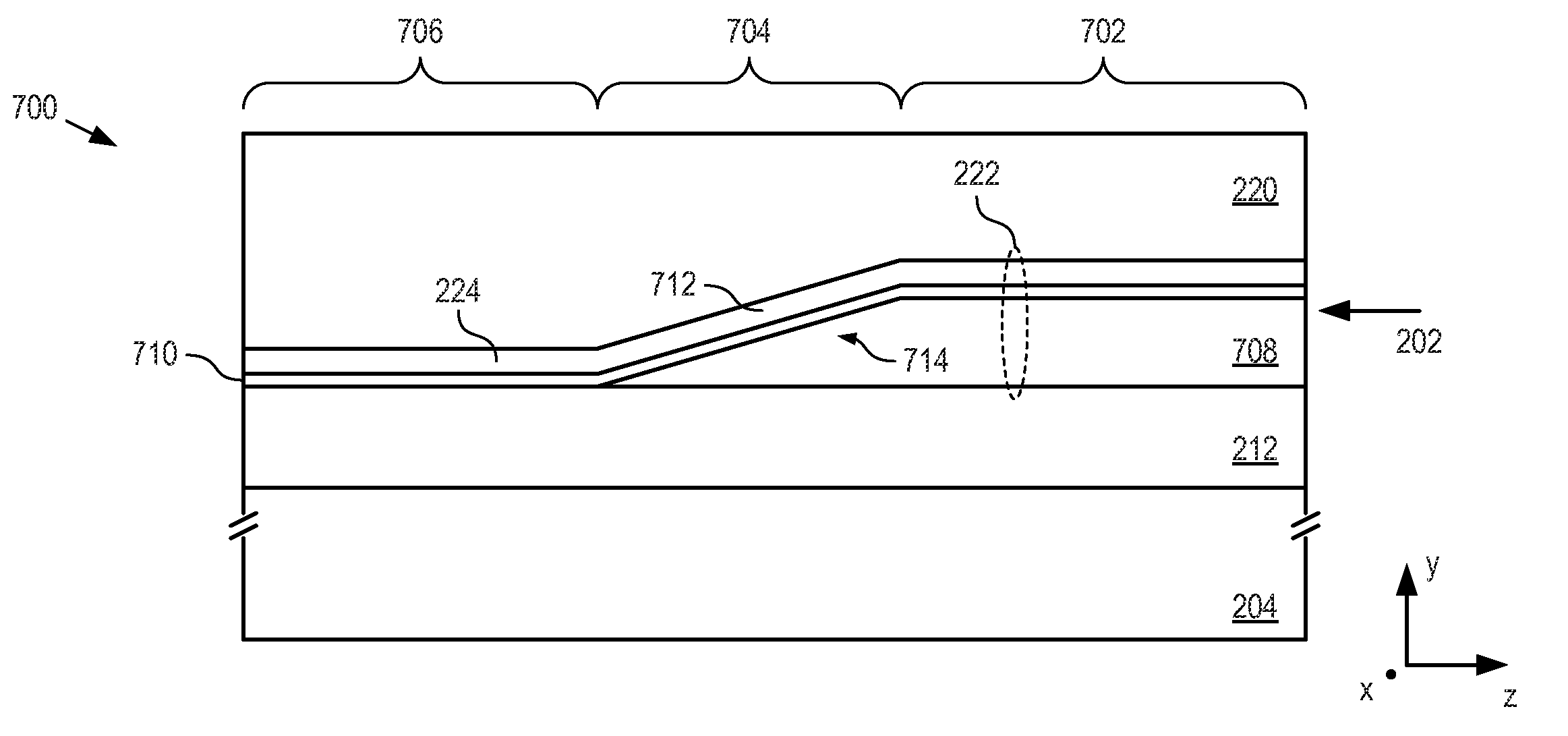
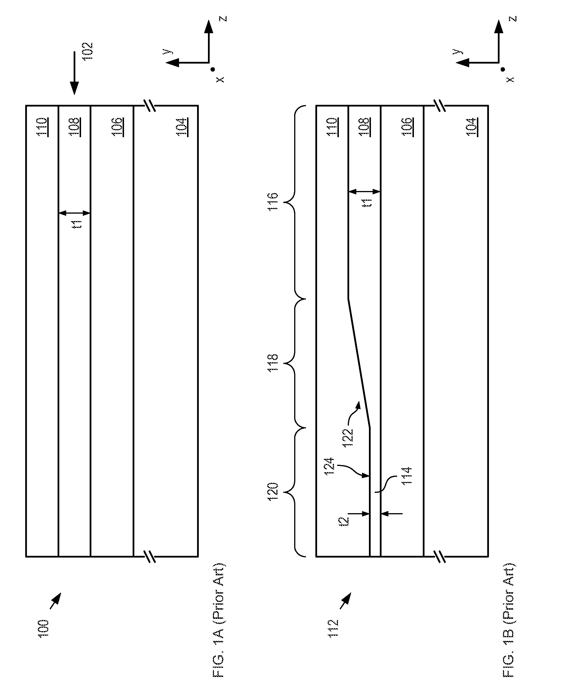
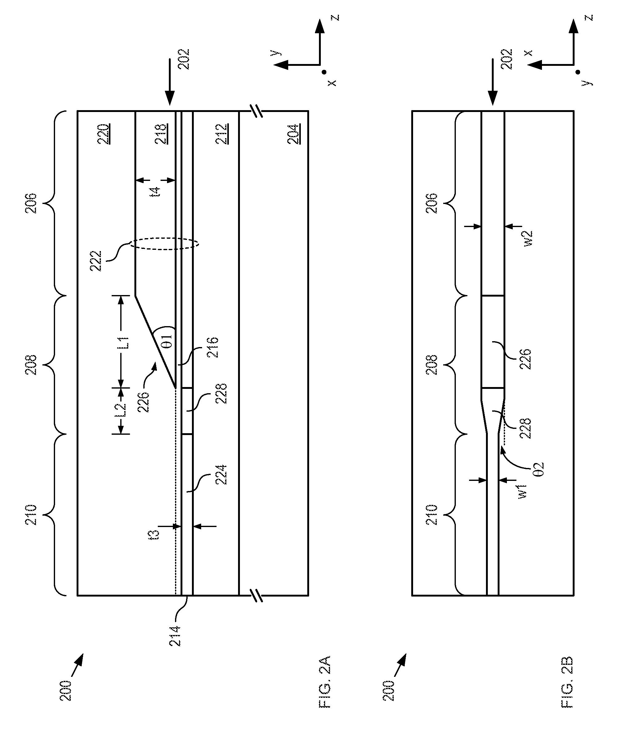
[0033]FIG. 1A depicts a schematic drawing of a cross-sectional view of a conventional surface waveguide having a thick core layer in accordance with the prior art.

[0034]Waveguide 100 is a surface waveguide having a core that is patterned to define a stripe (hereinafter referred to as a “stripe waveguide”). Waveguide 100 comprises lower cladding 106, core layer 108, and upper cladding 110, which are formed on substrate 104. For the purposes of the present Specification, including the appended claims, the terms “Disposed on” or “Formed on” are defined as “exists on or above” an underlying material or layer either in direct physical contact or with one or more intervening layers. For example, if a material is described to be “disposed (or grown) on a substrate,” this can mean that either (1) the material is in intimate contact with the substrate; or (2) the material is in contact with one or more layers that already reside on the substrate.

[0035]Each of lower cladding layer 106 and upp...


PUM


Abstract

A method for forming a waveguide having a thin-core region, a thick-core region, and a transition region of tapered thickness between them is disclosed. The method comprises forming a lower core layer of a first material on a lower cladding, forming a thin central core layer of a second material on the first core layer, forming an upper core layer of the first material on the central core layer, and etching the upper core layer in an etchant such that it is removed from the thin-core region and its thickness monotonically changes from its as-deposited thickness to extinction across the transition region, where the central core layer protects the lower core layer from exposure to the etchant.

Description

CROSS REFERENCE TO RELATED APPLICATIONS[0001]This case claims priority of U.S. Provisional Patent Application Ser. No. 61 / 712,587, filed Oct. 11, 2012, which is incorporated by reference.[0002]In addition, the underlying concepts, but not necessarily the language, of the following cases are incorporated by reference:[0003](1) U.S. Pat. No. 7,146,087, issued Dec. 5, 2006; and[0004](2) U.S. Pat. No. 7,142,759, issued Nov. 28, 2006.[0005]If there are any contradictions or inconsistencies in language between this application and one or more of the cases that have been incorporated by reference that might affect the interpretation of the claims in this case, the claims in this case should be interpreted to be consistent with the language in this case.FIELD OF THE INVENTION[0006]The present invention relates to integrated optics in general, and, more particularly, to surface waveguide structure and technology.BACKGROUND OF THE INVENTION[0007]Planar Lightwave Circuits (PLCs) are optical sy...

Claims


Application Information

Patent Timeline
Patent Type & Authority Patents(United States)
IPC IPC(8): G02B6/10G02B6/14G02B6/30
CPCG02B6/305G02B6/14
Inventor HEIDEMAN, RENE GERRITLEINSE, ARNE
Owner OCTROLIX
Why Eureka
Try Eureka