Method for forming conformal, homogeneous dielectric film by cyclic deposition and heat treatment

a dielectric film, homogeneous technology, applied in the direction of coatings, chemical vapor deposition coatings, metallic material coating processes, etc., can solve the problems of poor conformality or poor step coverage on a substrate containing small and/or high aspect ratio features, poor film quality and wet etch rate along sidewalls of trenches and holes relative to those of top/bottom surfaces of trenches and holes

Active Publication Date: 2015-05-05
ASM IP HLDG BV
View PDF9 Cites 401 Cited by
  • Summary
  • Abstract
  • Description
  • Claims
  • Application Information

AI Technical Summary

Problems solved by technology

However, the PECVD method for forming silicon nitride leads to poor conformality or poor step coverage on a substrate containing small and / or high aspect ratio features.
In small circuits and devices, such as ultra-large scale integrated (ULSI) circuitry, poor conformal coverage can hamper the development of higher density circuit devices and elements.
However, the present inventors have discovered that although cyclic deposition methods improve conformality of films, the film qualities such as wet etch rate are poor along sidewalls of trenches and holes relative to those of top / bottom surfaces of trenches and holes, especially when the trenches and holes are small (e.g., about 10 nm to about 50 nm in width) and / or have a high aspect ratio (e.g., about 5 to about 20).
The present inventors believe that that is because when trenches and holes are small and / or have a high aspect ratio, deposition reactions do not sufficiently progress on sidewalls even if high conformality of films is achieved, and as a result, impurities remain inside the films as residues of reaction gases and / or byproducts of reaction.

Method used


Image

  • Method for forming conformal, homogeneous dielectric film by cyclic deposition and heat treatment
  • Method for forming conformal, homogeneous dielectric film by cyclic deposition and heat treatment
  • Method for forming conformal, homogeneous dielectric film by cyclic deposition and heat treatment

Examples


examples

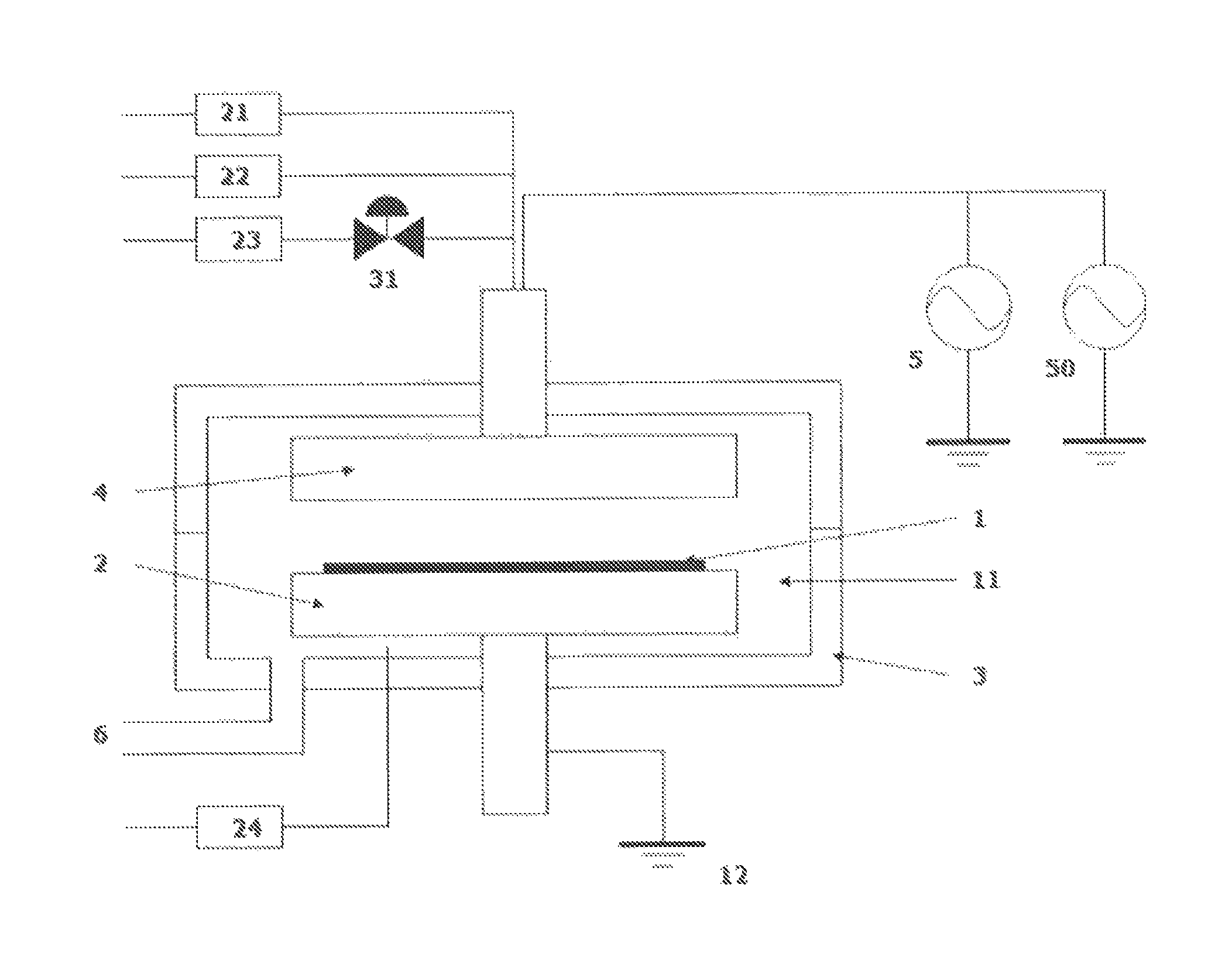
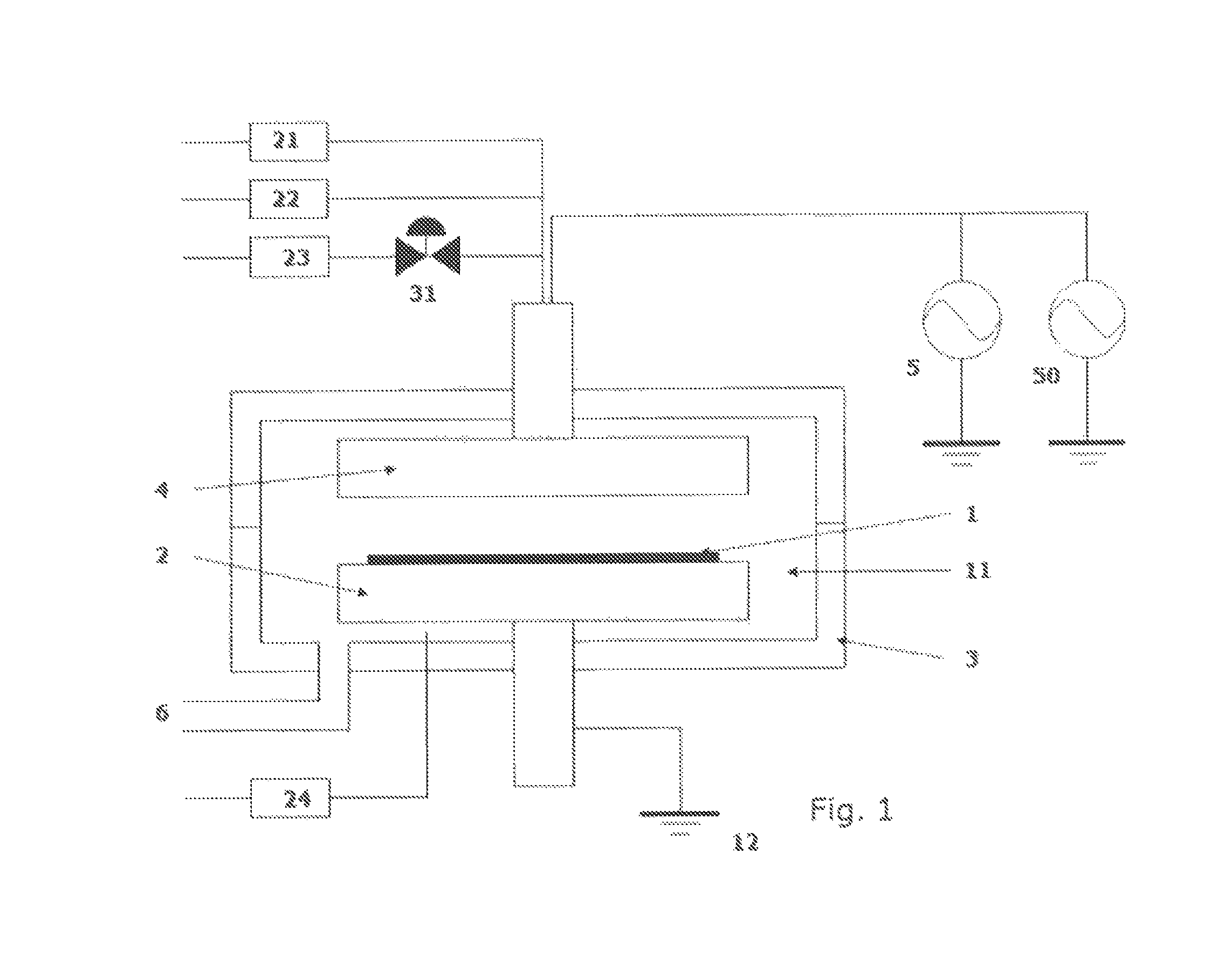
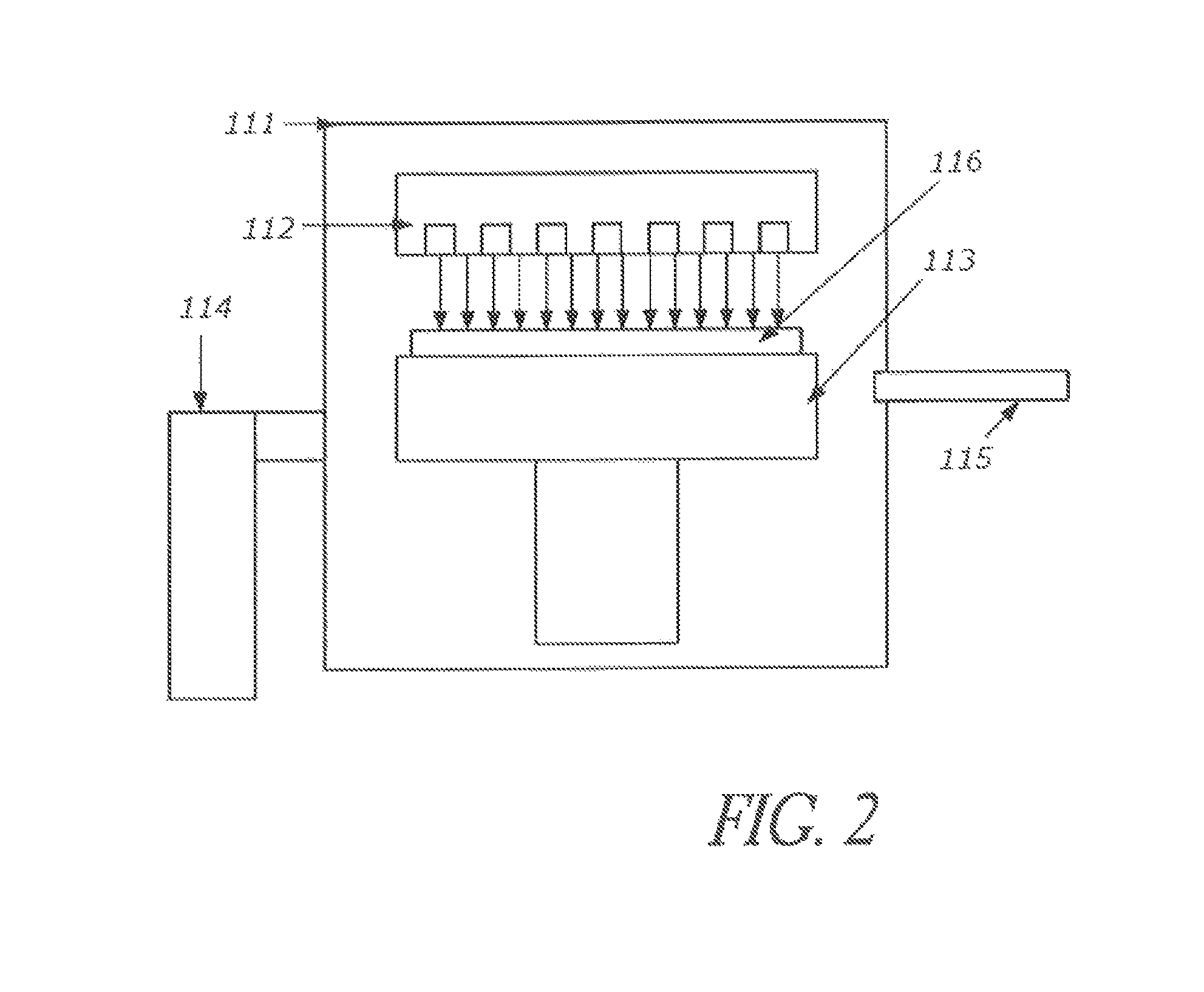
[0052]Film A and film B (SiNH dielectric films) were each formed on a 300-mm substrate having a patterned surface having an aspect ratio of about 2 and an opening width of about 50 nm under the conditions shown below using the PEALD apparatus illustrated in FIG. 1. The thickness of film was 30 nm for evaluating film properties.

Film A by PEALD:

[0053]Precursor: 1,2-dichloro-tetramethyl-disilane

[0054]Precursor inflow pressure: 665 Pa (Vapor Pressure)

[0055]Carrier gas flow: Ar at 2 SLM

[0056]Reactant gas flow (continuous): NH3 at 2 SLM

[0057]Purge gas flow: He at 500 sccm

[0058]Substrate temperature: 400° C.

[0059]RF frequency: 13.56 MHz

[0060]RF power: 400 W

[0061]Precursor supply time: 2 seconds

[0062]Purge time after precursor pulse: 1 second

[0063]RF Plasma exciting time: 3 seconds

[0064]Purge time after RF application: 1 second

[0065]Number of cycles: 500 times

Film B by PE-ALD:

[0066]Precursor: Tetrakis-ethylamino-silane

[0067]Precursor inflow pressure: 300 Pa (Vapor Pressure)

[0068]Carrier gas...


PUM

PropertyMeasurementUnit
temperatureaaaaaaaaaa
temperaturesaaaaaaaaaa
aspect ratioaaaaaaaaaa

Abstract

A method for forming a conformal, homogeneous dielectric film includes: forming a conformal dielectric film in trenches and / or holes of a substrate by cyclic deposition using a gas containing a silicon and a carbon, nitrogen, halogen, hydrogen, and / or oxygen, in the absence of a porogen gas; and heat-treating the conformal dielectric film and continuing the heat-treatment beyond a point where substantially all unwanted carbons are removed from the film and further continuing the heat-treatment to render substantially homogeneous film properties of a portion of the film deposited on side walls of the trenches and / or holes and a portion of the film deposited on top and bottom surfaces of the trenches and / or holes.

Description

CROSS-REFERENCE TO RELATED APPLICATIONS[0001]This application claims priority to U.S. Provisional Patent Application No. 61 / 670,496, entitled “Method for Forming Conformal, Homogeneous Dielectric Film by Cyclic Deposition and Heat Treatment,” and filed on Jul. 11, 2012, all of which is incorporated herein by reference.BACKGROUND OF THE INVENTION[0002]1. Field of the Invention[0003]The present invention generally relates to semiconductor integrated circuit manufacturing and, more particularly to a method of forming a conformal, homogeneous dielectric film such as a silicon nitride film by cyclic deposition, such as atomic layer deposition, and heat treatment.[0004]2. Description of the Related Art[0005]Integrated circuits fabricated on semiconductor substrates for large scale integration require multiple levels of metal interconnections to electrically interconnect discrete layers of semiconductor devices formed on semiconductor chips. The different levels of interconnections are sep...

Claims


Application Information

Patent Timeline
Patent Type & Authority Patents(United States)
IPC IPC(8): H01L21/31H01L21/469C23C16/34C23C16/455C23C16/56H01L21/02
CPCC23C16/45536C23C16/56H01L21/02318H01L21/02164H01L21/0217H01L21/02211H01L21/02219H01L21/02274H01L21/0228H01L21/02348C23C16/345
Inventor BEYNET, JULIENRAAIJMAKERS, IVOFUKAZAWA, ATSUKI
Owner ASM IP HLDG BV
Why Eureka
Try Eureka