Semiconductor structure having a metal gate with side wall spacers

a metal gate and semiconductor technology, applied in the direction of basic electric elements, electrical equipment, semiconductor devices, etc., can solve the problems of high electrical resistance low operation speed of poly-silicon gate electrodes with high electrical resistance with respect to metal conducting lines, and the integration process of semiconductor structures having metal gates has more challenges and problems. to achieve the effect of improving the problem of overhang

Active Publication Date: 2015-06-02
MARLIN SEMICON LTD
View PDF36 Cites 19 Cited by
  • Summary
  • Abstract
  • Description
  • Claims
  • Application Information

AI Technical Summary

Benefits of technology

[0008]One object of the present invention is to provide a semiconductor structure having a metal gate and a method of forming the same to improve the aforementioned problems.
[0011]The semiconductor structure having a metal gate electrode and the method of forming the same of the present invention mainly utilizes the broadened opening formed by removing a portion of the first spacer to fulfill the fabrication of the gate conductive layer via the broadened opening. The semiconductor structure having a metal gate and the method of forming the same of the present invention may efficiently improve the overhang problem of the conventional metal gate fabrication, such that the problems of overhang or void are overcome when the gate conductive layer fills the well of the gate structure, such that the gate conductive layer may cover the inner wall of the gate structure uniformly and continuously. Also, the problems of overhang or void in the well may be solved.

Problems solved by technology

On the contrary, the poly-silicon gate still has many disadvantages which may not be conquered until now.
Firstly, as compared with the poly-silicon material and most metal materials, poly-silicon material is a kind of semiconductor material having high electrical resistance, such that the operational speed of the poly-silicon gate electrode having high electrical resistance is still low with respect to the metal conducting line.
However, since line width of the semiconductor structure is minimized to a limitation, the integration process of the semiconductor structure having a metal gate has more challenges and problems.
Because the aspect ratio of the well 19 of the gate structure 12 of the semiconductor structure is a limitation especially when minimized to 28 nm, a preferred step converge is not provided according to the method of depositing the metal gate conductive layer nowadays, such that the problems of overhang or void may occur to seriously influence the filling quality of the gate conductive layer.
In view of this, the metal gate conductive layer of the conventional semiconductor structure having a metal gate has non-ideal drawbacks.
In addition, the problems of void and overhang may not be solved according to the present manufacturing techniques.

Method used


Image

  • Semiconductor structure having a metal gate with side wall spacers
  • Semiconductor structure having a metal gate with side wall spacers
  • Semiconductor structure having a metal gate with side wall spacers

Examples


Embodiment Construction

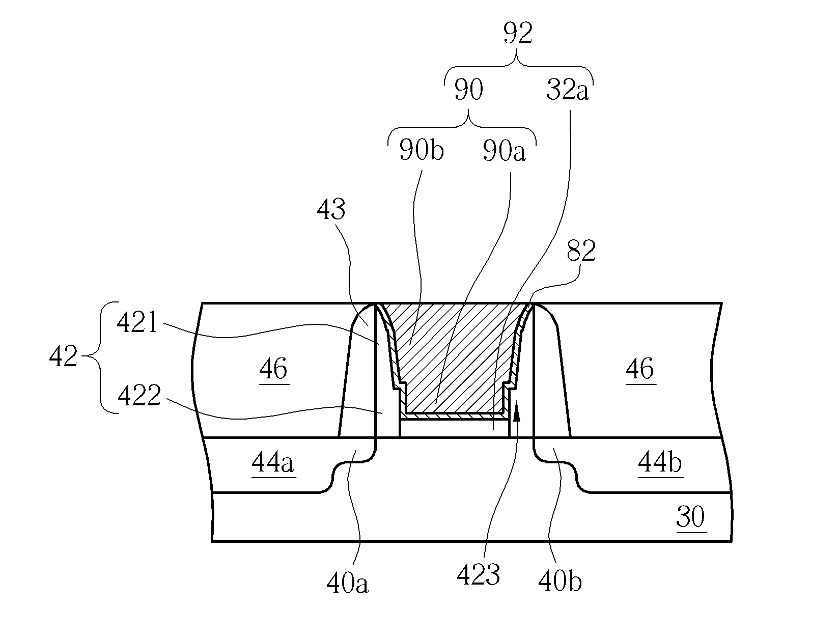
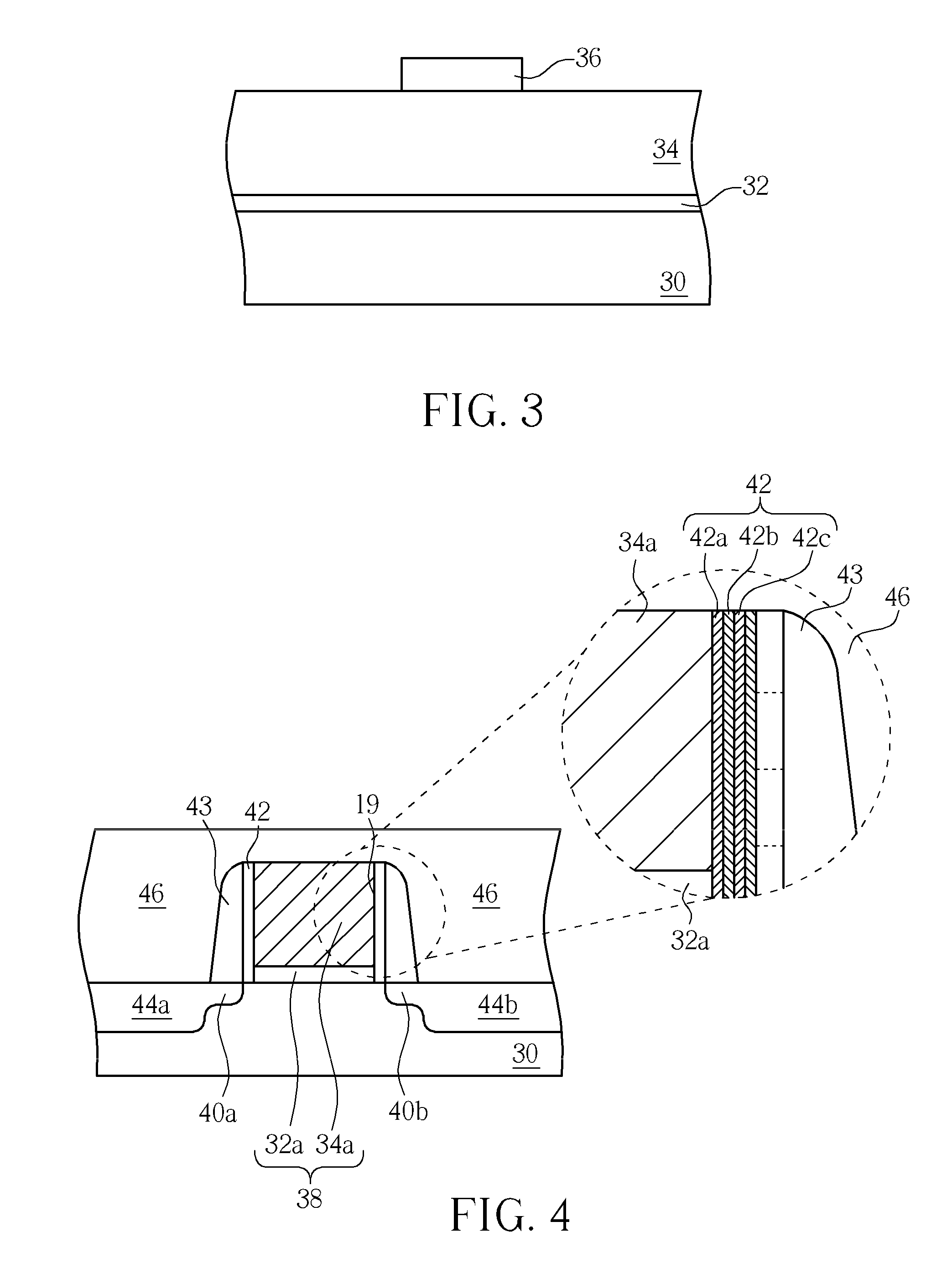
[0016]Please refer to FIG. 3 to FIG. 9, FIG. 3 and FIG. 9 are schematic diagrams illustrating the method of forming a semiconductor structure having a metal gate of the present invention. As illustrated in FIG. 3, firstly, a semiconductor substrate is provided 30, and the material of the semiconductor substrate 30 may include silicon, silicon germanium (SiGe), epitaxy silicon or epitaxy germanium. Afterwards, a dielectric layer 32 and a poly-silicon layer 34 are sequentially formed on the semiconductor substrate 30, and the material of the poly-silicon layer 34 is made of the poly-silicon material which are undoped or having N+ or P+ dopants. Afterwards, a shielding layer (not shown in figure) is formed on the poly-silicon layer 34. Also, a patterned photoresist layer (not shown in figure) serves as a mask to perform a pattern process to form a patterned shielding layer 36. In addition, the patterned shielding layer 36 is made of silicon oxide (SiO2), silicon nitride (SiN), silicon ...


PUM


Abstract

A method of forming a semiconductor structure having a metal gate. Firstly, a semiconductor substrate is provided. Subsequently, at least a gate structure is formed on the semiconductor substrate. Afterwards, a spacer structure is formed to surround the gate structure. Then, an interlayer dielectric is formed. Afterwards, a planarization process is performed for the interlayer dielectric. Then, a portion of the sacrificial layer is removed to form an initial etching depth, such that an opening is formed to expose a portion of the spacer structure. The portion of the spacer structure exposed to the opening is removed so as to broaden the opening. Afterwards, remove the sacrificial layer completely via the opening. Finally, a gate conductive layer is formed to fill the opening.

Description

BACKGROUND OF THE INVENTION[0001]1. Field of the Invention[0002]The present invention relates to a semiconductor structure having a metal gate and a method of forming the same, and more particular to a semiconductor structure having a broadened opening and a method of forming the same.[0003]2. Description of the Prior Art[0004]The performance of semiconductors has increased year after year with the critical dimensions and the advance of large-scale integrated circuits. In the field of semiconductor fabrication, since poly-silicon material has a strong heat resistance, the poly-silicon material is commonly used to fabricate the gate structure of the semiconductor structure, especially for the fabrication of the gate electrode of the metal oxide semiconductor transistor. In addition, the gate electrode made of poly-silicon may prevent dopings into the channel region during the ion implantation process. In addition, in the high-temperature environment, the poly-silicon gate electrode m...

Claims


Application Information

Patent Timeline
Patent Type & Authority Patents(United States)
IPC IPC(8): H01L29/66H01L21/28H01L29/78H01L29/423H01L29/49
CPCH01L29/6656H01L21/28114H01L29/42372H01L29/42376H01L29/495H01L29/4983H01L29/66545H01L29/66583H01L29/7833H01L29/40114H01L21/2633H01L21/28026H01L29/6653
Inventor CHEN, YI-WEIHO, NIEN-TINGHUANG, CHIEN-CHUNGLIN, CHIN-FU
Owner MARLIN SEMICON LTD
Why Eureka
Try Eureka