Semiconductor device having through-substrate via with insulating portion

a technology of through-substrate via and insulating portion, which is applied in the direction of semiconductor devices, semiconductor/solid-state device details, electrical apparatus, etc., can solve the problems of large voids and dust emission, and achieve the effect of reducing dust emission and increasing fabrication yield

Active Publication Date: 2015-06-09
LONGITUDE LICENSING LTD
View PDF2 Cites 6 Cited by
  • Summary
  • Abstract
  • Description
  • Claims
  • Application Information

AI Technical Summary

Benefits of technology

[0013]According to an embodiment of the invention, since a slit, which has been formed on the upper portion of a first insulating film burying in an isolation portion, is buried with a second insulating film before CMP, it is possible to prevent components that are used in a CMP process, a material removed by polishing, and other residues from remaining in the slit. Accordingly, it is possible to reduce the dust emission in the subsequent process. As a result, it is possible to increase the yield of the fabrication of a semiconductor device that has a TSV, which is provided with the isolation portion.

Problems solved by technology

In particular, when the silicon oxide film is deposited by a method having a poor coverage, the opening of the TSV trench is closed first, thereby forming large voids.
Such residues may become a cause for dust emission that may occur in the subsequent process.

Method used


Image

  • Semiconductor device having through-substrate via with insulating portion
  • Semiconductor device having through-substrate via with insulating portion
  • Semiconductor device having through-substrate via with insulating portion

Examples


first exemplary embodiment

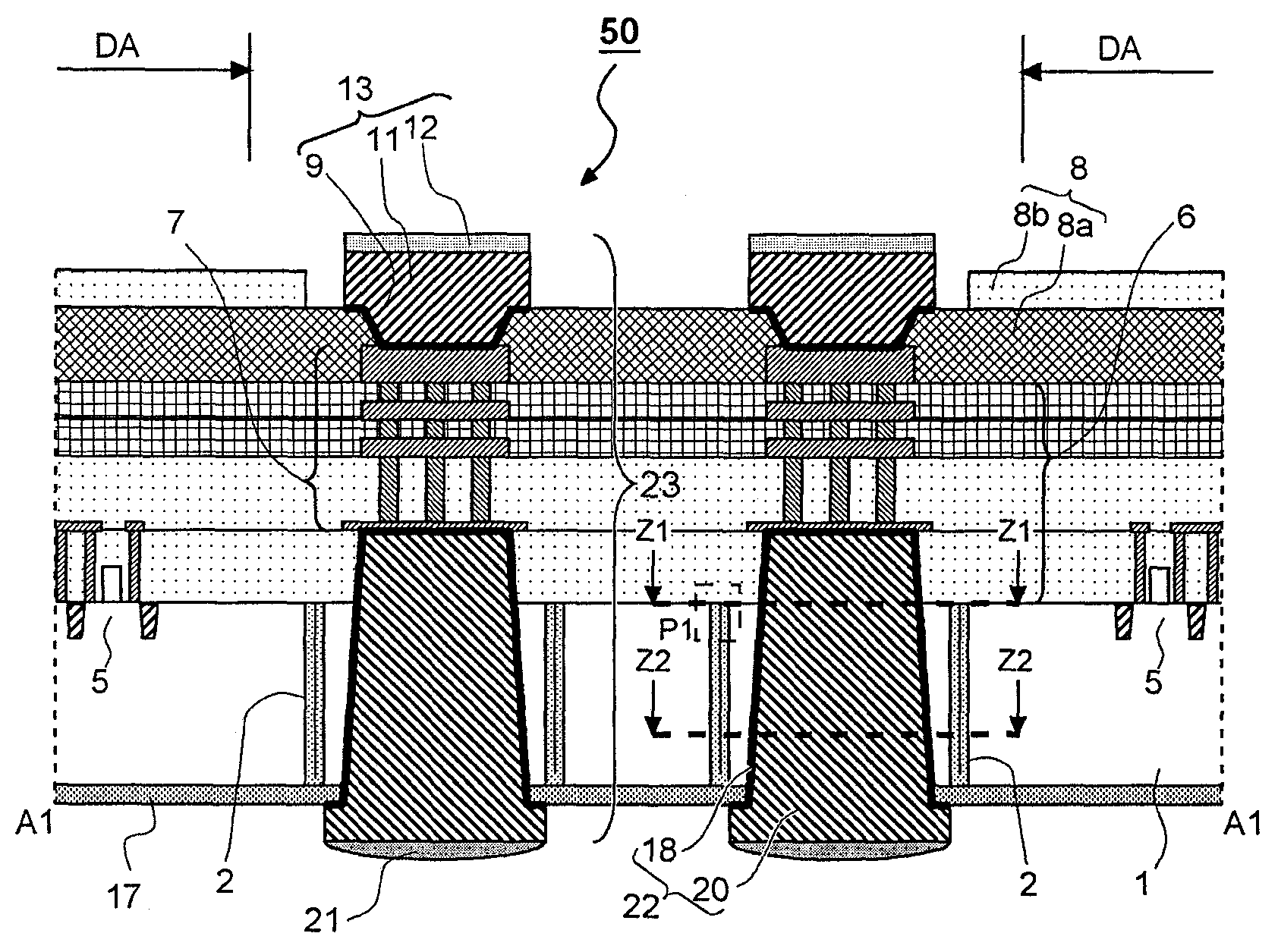
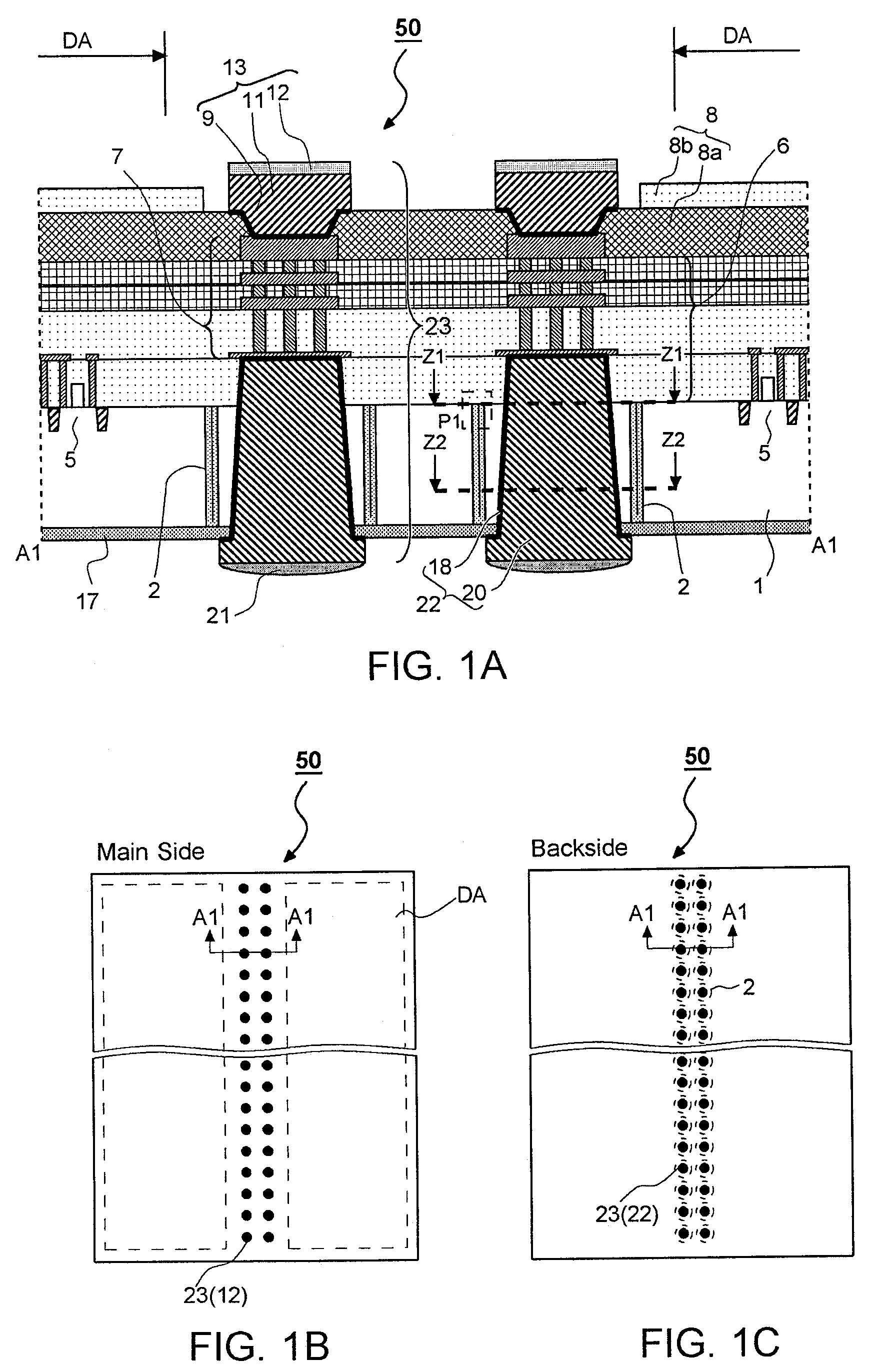
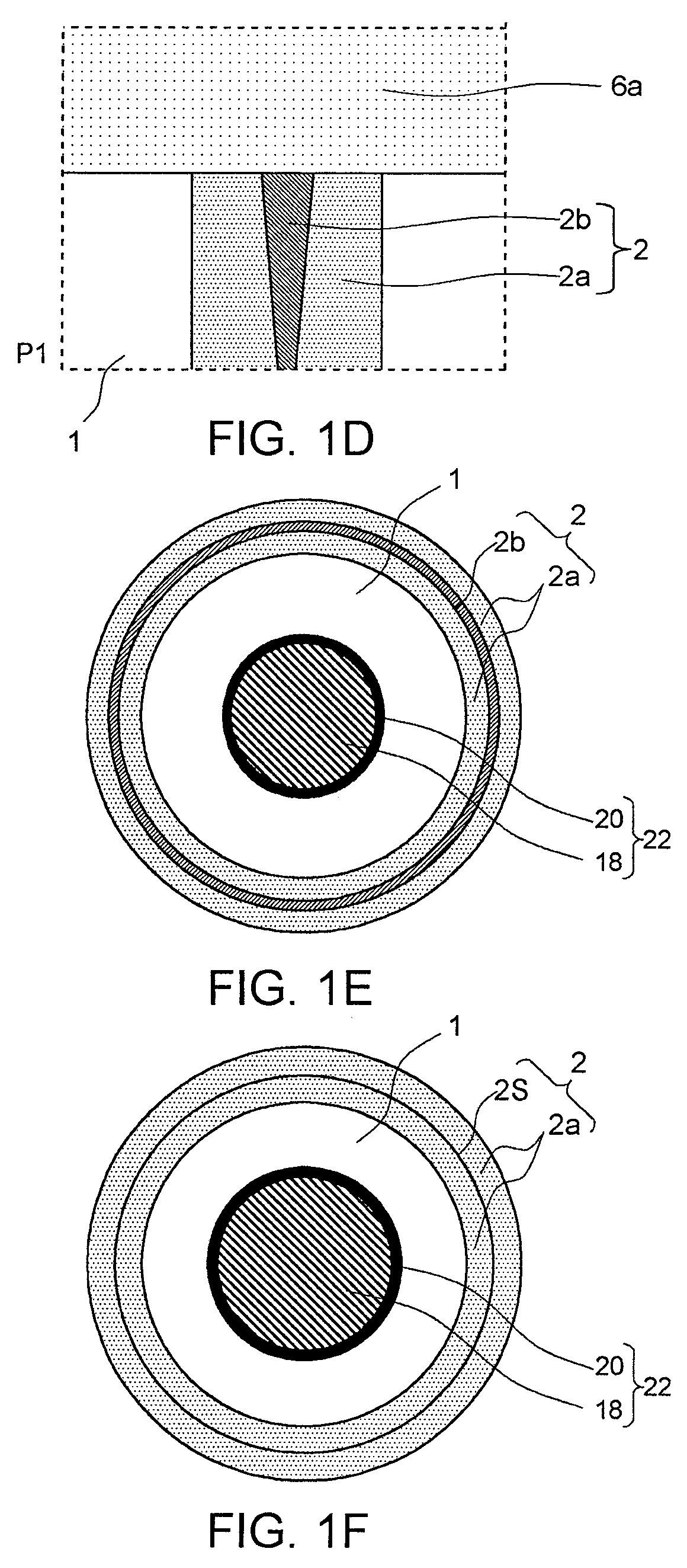
[0026]FIG. 1 depicts an example of a semiconductor device (semiconductor chip 50) having a TSV structure to which the invention is applied, in which FIG. 1A is a schematic cross-sectional view depicting a TSV structure part, FIG. 1B shows a top plan view at the side of the first surface, FIG. 1C is a top plan view at the side of the second surface. FIG. 1A corresponds to a cross-sectional view taken along A1-A1 line in FIG. 1B and FIG. 1C. FIG. 1D corresponds to an enlarged view of portion P1 of FIG. 1A, and FIG. 1E and FIG. 1F correspond to horizontal cross-sectional views taken along Z1-Z1 and Z2-Z2 lines in FIG. 1A, respectively.

[0027]A semiconductor substrate 1 is provided with isolation portions (referred to as an insulating ring) 2 that have an annular structure when viewed from above. Each insulating ring 2 insulates and separates a first semiconductor area (TSV forming area) from a second semiconductor area (device area DA). The TSV 22, which is composed of a seed layer 18 a...

modified example 1

[0049]In addition, although the insulating ring 2 is illustrated as having a single ring structure in the first exemplary embodiment, this is not intended to be limiting. Rather, the insulating ring 2 may have a multiple ring structure. In an example, FIG. 12A is a schematic cross-sectional view of a semiconductor chip 60 that has a double-ring structure, FIG. 12B shows a partially-enlarged view of part P2, and FIG. 12C shows a cross-sectional view along Z1-Z1 line in FIG. 12A. The insulating ring includes an inner insulating ring 2A and an outer insulating ring 2B. In each surface, the second insulating film 2b is formed in a groove-shaped slit (hole) in the middle of the width of the insulating ring.

modified example 2

[0050]In the foregoing embodiment, a vertical trench (TSV trench) 2T is formed as the shape of the trench for the insulating ring. However, in response to recent miniaturization of semiconductor devices, the size of the opening of the TSV trench tends to decrease and the aspect ratio of the opening tends to increase further. Because of this, when the first insulating film 2a is filled in the vertical TSV trench by CVD, the first insulating films 2a, which are deposited on the upper portion of the opening, come into contact with each other, so that cavities (voids) tend to remain in the lower portion. When such voids are created, the bonding force in a seam 2S tends to be decreased, and the area surrounded by the insulating ring tends to be isolated. This tends to be a reason by which cracks or the like occur in the interlayer insulating film 6 or the like in the subsequent manufacturing process. Therefore, it is effective to process the upper portion of the opening of the TSV trench...


PUM


Abstract

A semiconductor device includes an isolation portion penetrating a semiconductor substrate from a first surface to a second surface positioned opposite the first surface. The isolation portion includes a first insulating film and a second insulating film. The first insulating film has a slit portion at a side of the first surface and the slit portion is buried with the second insulating film. The semiconductor device further includes an electrode penetrating the semiconductor substrate that is surrounded by the isolation portion.

Description

BACKGROUND OF THE INVENTION[0001]1. Field of the Invention[0002]The present invention relates to a semiconductor device, and more particularly, to a semiconductor device having an electrode that extends through a semiconductor substrate.[0003]2. Description of the Related Art[0004]Recently, in response to the high functionality and diversification of semiconductor devices, a semiconductor device that is integrated by stacking a plurality of semiconductor chips in the vertical direction is being proposed. This semiconductor device is designed such that an electrical connection between respective semiconductor chips is formed by a through silicon via (referred to as TSV), which penetrates through the semiconductor substrate of the respective semiconductor chip.[0005]In the meantime, since the TSV is formed so as to extend through the semiconductor substrate, it is required to be designed so that the TSV is insulated from the semiconductor substrate. Therefore, an annular insulating-se...

Claims


Application Information

Patent Timeline
Patent Type & Authority Patents(United States)
IPC IPC(8): H01L29/00H01L23/48H01L23/00H01L21/768H01L25/065
CPCH01L23/481H01L24/13H01L24/14H01L21/76898H01L2224/16145H01L2224/13021H01L2224/1412H01L2224/14181H01L2224/32145H01L2224/32225H01L2224/73204H01L2924/15311H01L25/0657H01L2225/06513H01L2225/06541H01L2225/06565H01L2224/13009H01L2924/00H01L2924/351H01L2924/181
Inventor NAKAMURA, NOBUYUKIMURAMOTO, TAKUYUKITSUKAMOTO, TAKEO
Owner LONGITUDE LICENSING LTD
Why Eureka
Try Eureka