Semiconductor device including a gate electrode on a protruding group III-V material layer and method of manufacturing the semiconductor device

a technology of semiconductor devices and gate electrodes, which is applied in the direction of semiconductor devices, basic electric elements, electrical equipment, etc., can solve the problems of increasing the difficulty of maintaining or improving the performance of transistors, and achieve the effects of preventing the dispersion of carriers, small effective mass of electrons, and fast injection velocity

Active Publication Date: 2015-06-30
SAMSUNG ELECTRONICS CO LTD
View PDF52 Cites 13 Cited by
  • Summary
  • Abstract
  • Description
  • Claims
  • Application Information

AI Technical Summary

Benefits of technology

[0035]The semiconductor device according to the present invention includes a group III-V compound semiconductor material as a channel material, the group III-V compound semiconductor material having a small effective mass of electrons and fast injection velocity in a low electric field. The side and upper surfaces of a channel layer formed of the channel material are covered with a barrier layer having a bandgap larger than that of the channel material. Thus, dispersion of carriers may be prevented when carriers move in a channel, and thus, it is possible to move carriers at low power and high speed.
[0036]In addition, since the side and upper surfaces of the channel layer which contact a gate electrode are covered with the barrier layer having a large bandgap, the trap density at the interface of the channel layer is small compared to the case when the barrier layer does not exist or when the barrier layer partially exists. Thus, the degradation of characteristics of the semiconductor device which may occur when a voltage lower than a threshold voltage (sub-threshold swing) is applied thereto may be decreased.

Problems solved by technology

As semiconductor devices have become increasingly more highly integrated, it is increasingly more difficult to maintain or improve the performance of transistors due to reduction of the physical lengths of their gates.

Method used


Image

  • Semiconductor device including a gate electrode on a protruding group III-V material layer and method of manufacturing the semiconductor device
  • Semiconductor device including a gate electrode on a protruding group III-V material layer and method of manufacturing the semiconductor device
  • Semiconductor device including a gate electrode on a protruding group III-V material layer and method of manufacturing the semiconductor device

Examples


Embodiment Construction

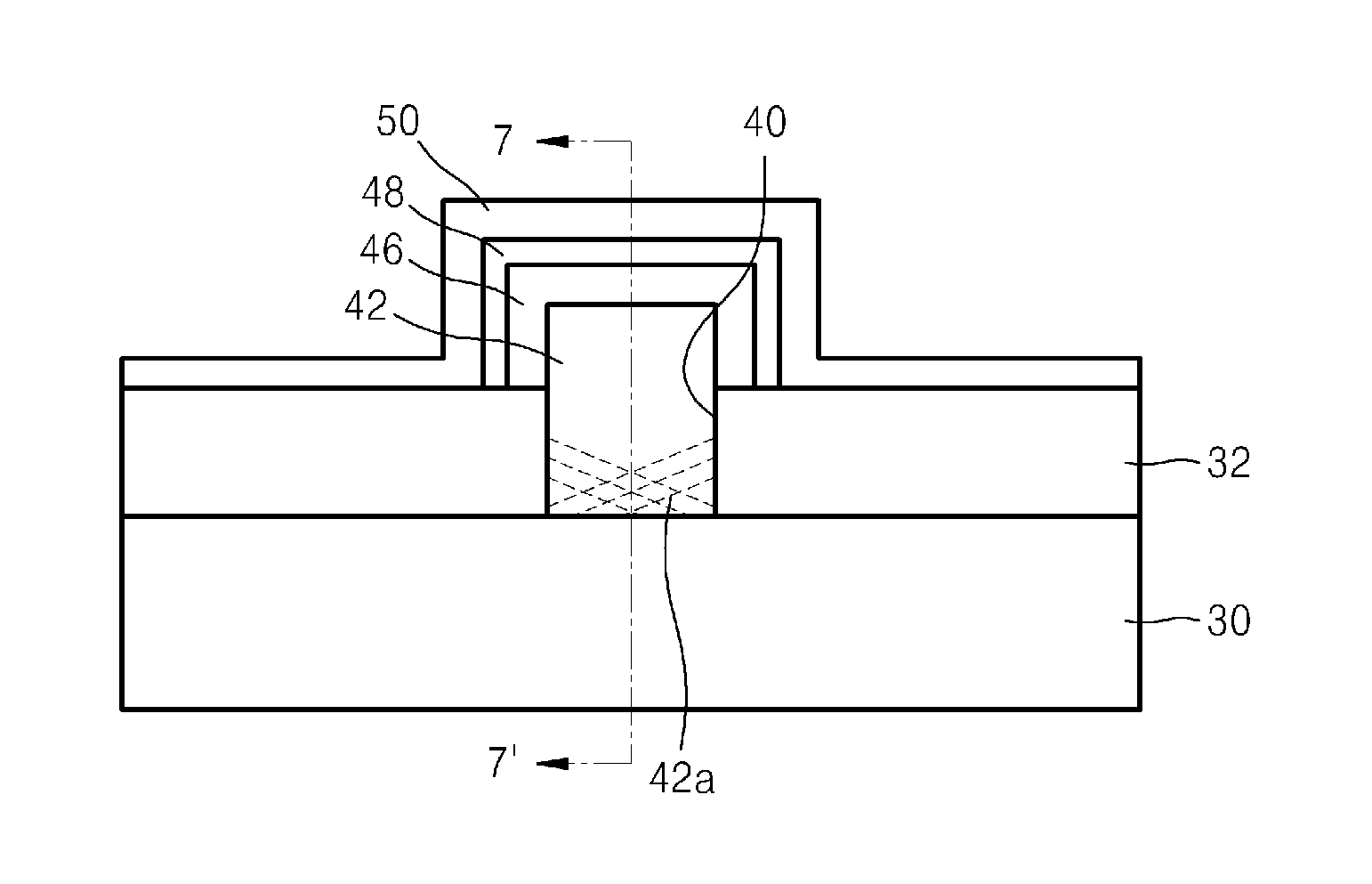
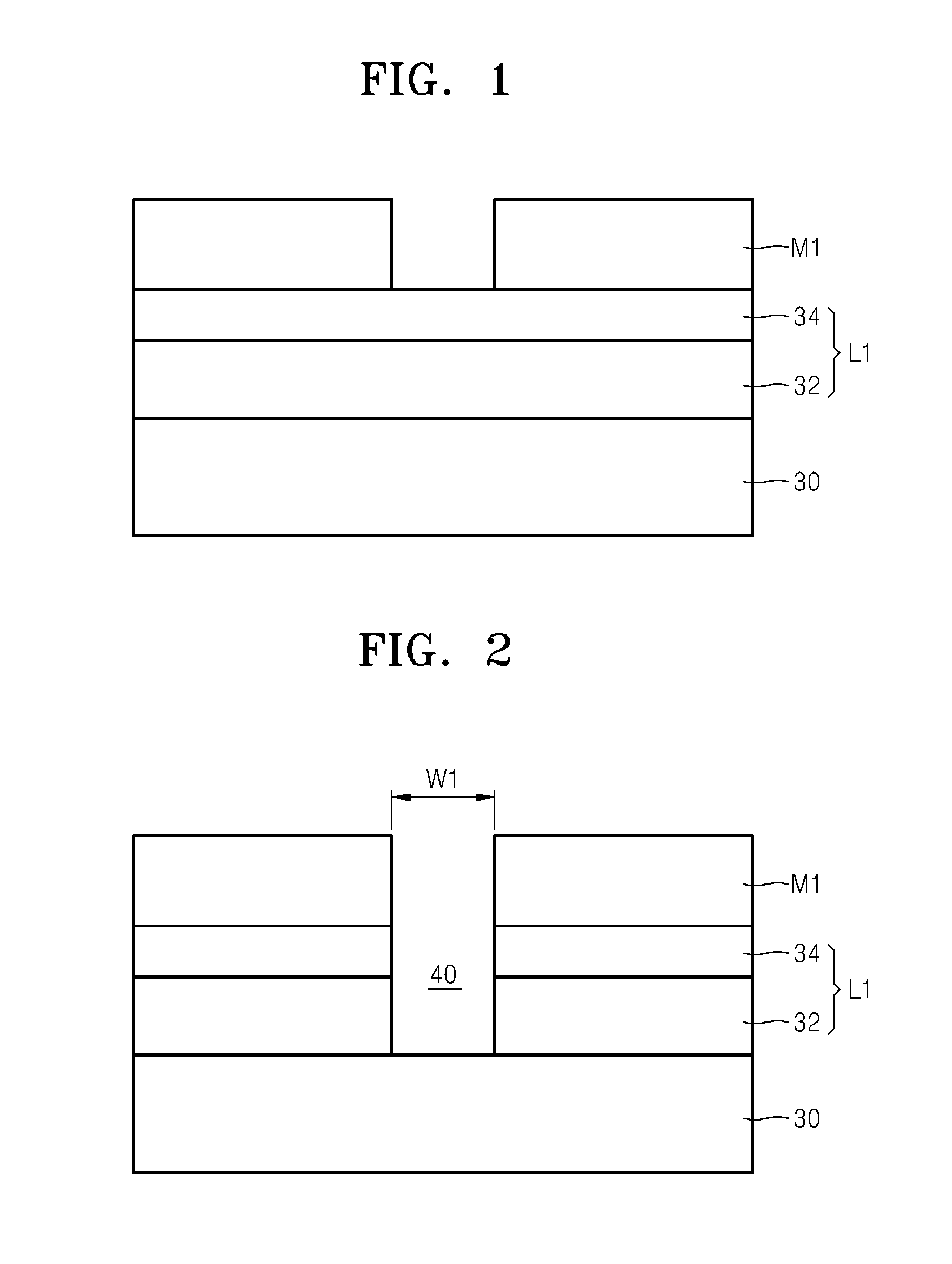
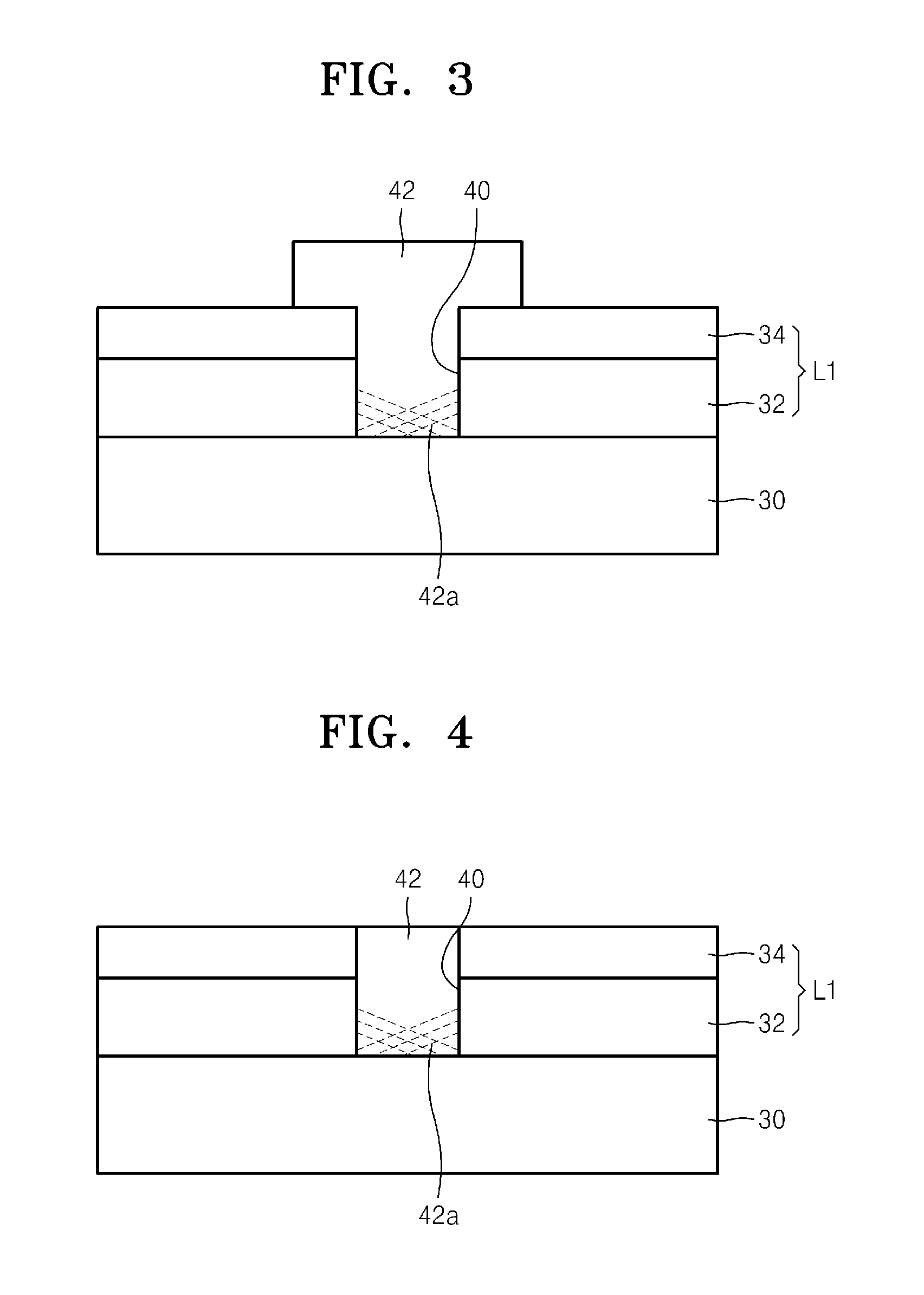
[0042]Reference will now be made in detail to embodiments, examples of which are illustrated in the accompanying drawings, wherein like reference numerals refer to like elements throughout. In this regard, the present embodiments may have different forms and should not be construed as being limited to the descriptions set forth herein. Accordingly, the embodiments are merely described below, by referring to the figures, to explain aspects of the present description.

[0043]The present invention now will be described more fully hereinafter with reference to the accompanying drawings, in which embodiments of the invention are shown. This invention may, however, be embodied in many different forms and should not be construed as limited to the embodiments set forth herein. In the drawings, the size and relative sizes of layers and regions may be exaggerated for clarity. Like reference numerals refer to like elements throughout.

[0044]It will be understood that when an element is referred t...


PUM

PropertyMeasurementUnit
thicknessaaaaaaaaaa
gate lengthsaaaaaaaaaa
width W1aaaaaaaaaa

Abstract

A semiconductor device including a group III-V barrier and a method of manufacturing the semiconductor device, the semiconductor device including: a substrate, insulation layers formed to be spaced apart on the substrate, a group III-V material layer for filling the space between the insulation layers and having a portion protruding higher than the insulation layers, a barrier layer for covering the side and upper surfaces of the protruding portion of the group III-V material layer and having a bandgap larger than that of the group III-V material layer, a gate insulation film for covering the surface of the barrier layer, a gate electrode formed on the gate insulation film, and source and drain electrodes formed apart from the gate electrode. The overall composition of the group III-V material layer is uniform. The barrier layer may include a group III-V material for forming a quantum well.

Description

CROSS-REFERENCE TO RELATED APPLICATIONS[0001]This application claims the benefit of Korean Patent Application No. 10-2011-0119125, filed on Nov. 15, 2011, in the Korean Intellectual Property Office, the disclosure of which is incorporated herein in its entirety by reference.BACKGROUND[0002]1. Field[0003]The present disclosure relates to semiconductor devices, and more particularly, to semiconductor devices including a group III-V barrier and methods of manufacturing the semiconductor devices.[0004]2. Description of the Related Art[0005]As semiconductor devices have become increasingly more highly integrated, it is increasingly more difficult to maintain or improve the performance of transistors due to reduction of the physical lengths of their gates.[0006]Thus, research is being conducted on technology involved in improving the performance of transistors by constructing them using a strained silicon (Si) channel or by constructing transistors using materials including a high k oxide...

Claims


Application Information

Patent Timeline
Patent Type & Authority Patents(United States)
IPC IPC(8): H01L29/06H01L29/66H01L29/778H01L29/20
CPCH01L29/66462H01L29/7787H01L29/20H01L21/18H01L29/772H01L21/02538H01L29/122H01L29/127H01L29/158H01L29/205H01L29/42376H01L29/66431H01L29/66522H01L29/66795H01L29/7783H01L29/7784H01L29/785
Inventor CHO, YOUNG-JINKIM, KYOUNG-YEONLEE, SANG-MOONHONG, KI-HAHWANG, EUI-CHUL
Owner SAMSUNG ELECTRONICS CO LTD
Why Eureka
Try Eureka