Package for an optoelectronic semiconductor component and semiconductor component

a technology of optoelectronic semiconductors and semiconductor components, applied in the direction of semiconductor lasers, lasers, basic electric elements, etc., can solve the problem that metal packages are too costly for consumer market applications, and achieve the effect of simple and inexpensive production and good heat dissipation of semiconductor components

Active Publication Date: 2015-06-30
OSRAM OLED
View PDF22 Cites 3 Cited by
  • Summary
  • Abstract
  • Description
  • Claims
  • Application Information

AI Technical Summary

Benefits of technology

[0004]In one aspect, the invention provides a package for an optoelectronic semiconductor component which may be produced simply and inexpensively and simultaneously ensures good heat dissipation from the semiconductor component.

Problems solved by technology

However, due to their comparatively complicated structure, these metal packages are too costly for consumer market applications.

Method used


Image

  • Package for an optoelectronic semiconductor component and semiconductor component
  • Package for an optoelectronic semiconductor component and semiconductor component
  • Package for an optoelectronic semiconductor component and semiconductor component

Examples


Embodiment Construction

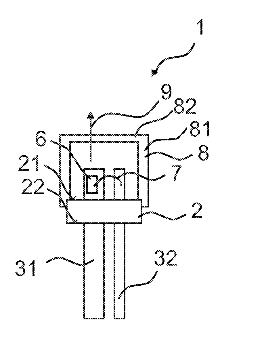
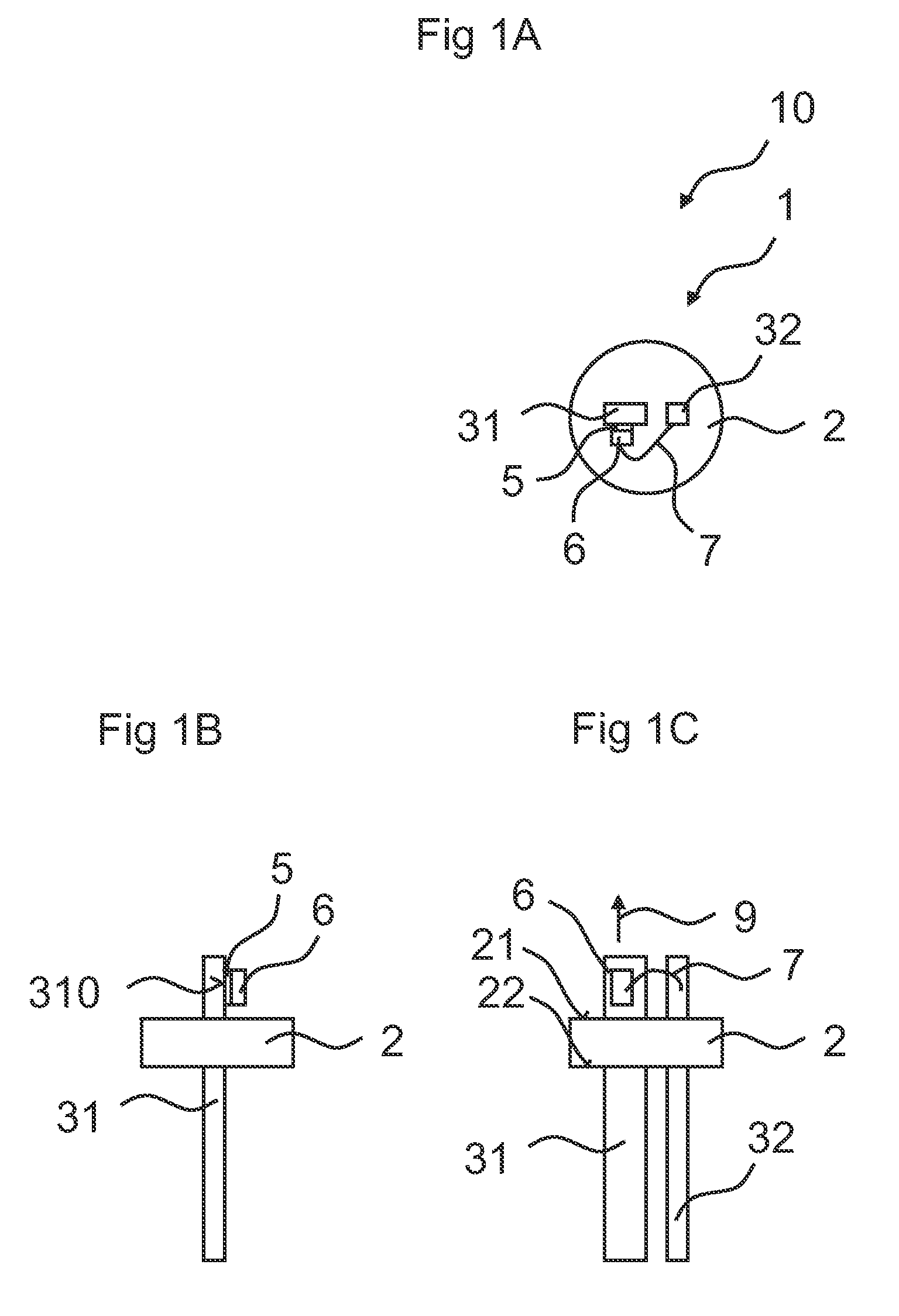
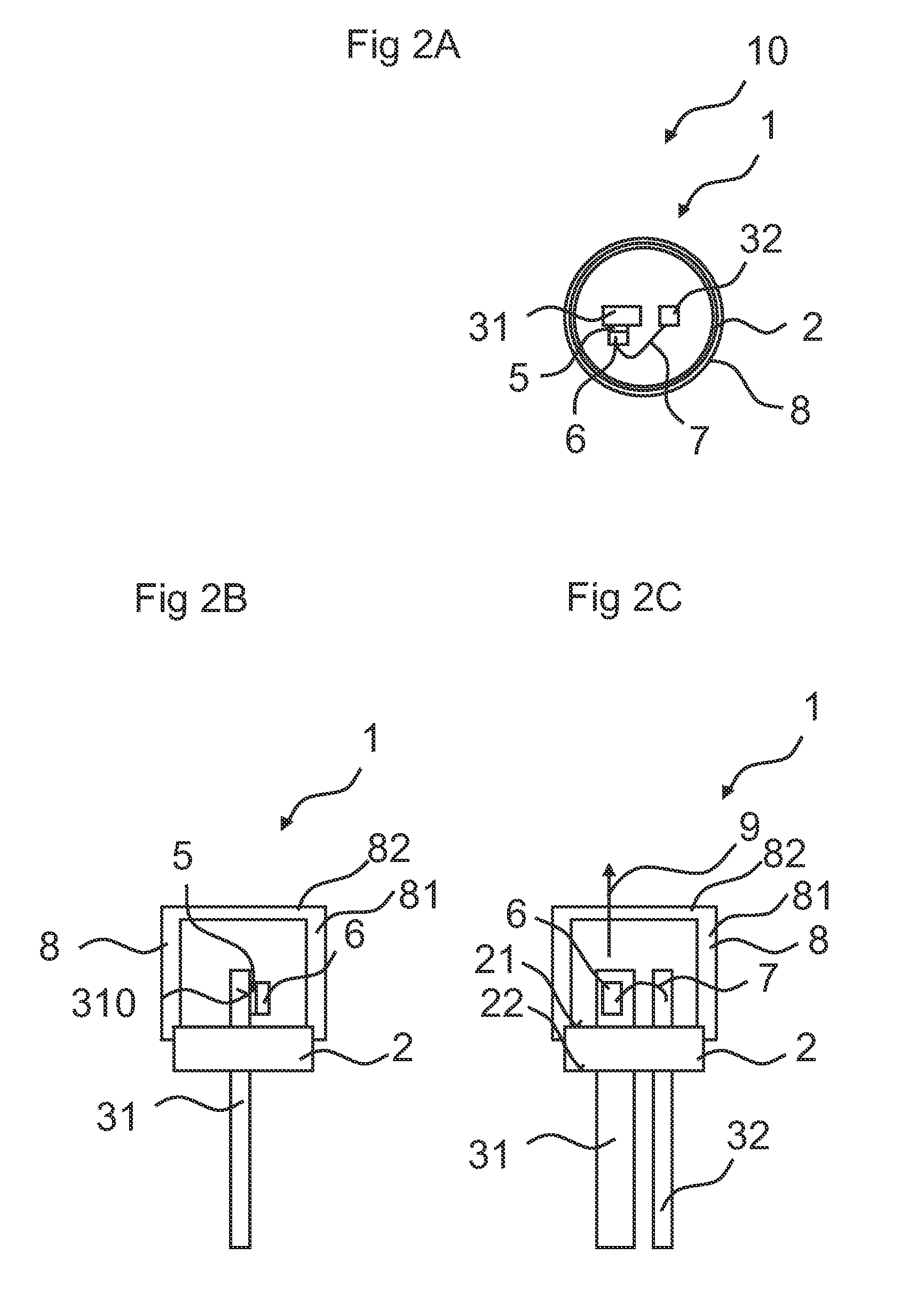
[0042]A first exemplary embodiment of a semiconductor component 10 with a package 1 and a semiconductor chip 6 fastened to the chip is illustrated schematically in FIGS. 1A to 1C. The package 1 comprises a package body 2, a first connecting lead 31 and a second connecting lead 32. The connecting leads form a lead frame for the package. The package body 2 has a first major face 21 and a second major face 22, between which the package body 2 extends in the vertical direction.

[0043]The first connecting lead 31 and the second connecting lead 32 extend parallel to one another and pass through the package body 2 in the vertical direction, in particular perpendicular to the first major face. A plane defined by the connecting leads thus extends perpendicularly to the first major face 21 of the package body. A side face 310, extending in a vertical direction, of the first connecting lead 31 forms a mounting face 310, to which the semiconductor chip 6 on the prefabricated package 1 is fastene...


PUM


Abstract

A package for an optoelectronic semiconductor component is disclosed. The package includes a package body, a first connecting lead and a second connecting lead. The first connecting lead and the second connecting lead each extend in a vertical direction through the package body. A semiconductor component with such a package and a semiconductor chip are also disclosed.

Description

[0001]This patent application is a national phase filing under section 371 of PCT / EP2011 / 065847, filed Sep. 13, 2011, which claims the priority of German patent application 10 2010 046 090.7, filed Sep. 20, 2010, each of which is incorporated herein by reference in its entirety.TECHNICAL FIELD[0002]The present application relates to a package for an optoelectronic semiconductor component and to a semiconductor component with such a package.BACKGROUND[0003]“TO” packages, for example, TO56, TO38 or TO9 packages, are often used for semiconductor laser diodes with waste heat outputs up to the watt range. However, due to their comparatively complicated structure, these metal packages are too costly for consumer market applications.SUMMARY OF THE INVENTION[0004]In one aspect, the invention provides a package for an optoelectronic semiconductor component which may be produced simply and inexpensively and simultaneously ensures good heat dissipation from the semiconductor component.[0005]Ac...

Claims


Application Information

Patent Timeline
Patent Type & Authority Patents(United States)
IPC IPC(8): H01L23/495H01L33/62H01S5/022H01L33/64H01S5/024H01L33/48
CPCH01L33/62H01L33/48H01L33/486H01S5/02272H01L33/483H01L33/647H01S5/02212H01S5/02469H01S5/0226H01S5/02276H01L2224/48091H01L2224/48247H01L2224/32245H01L2224/73265H01L2924/00012H01L2924/00H01S5/0236H01S5/02345H01L2924/00014H01S5/0237
Inventor MOELLMER, FRANKARZBERGER, MARKUSSCHWIND, MICHAELHOEFER, THOMAS
Owner OSRAM OLED
Why Eureka
Try Eureka