
Photoresist film and manufacturing method for organic light emitting display device using the same

a technology of photoresist film and organic light, applied in the direction of sustainable manufacturing/processing, thermography, instruments, etc., can solve the problems of reducing the functional efficiency of the light-emitting device exposed for the manufacturing process, the fmm method may have a problem of sagging mask, and the difficulty of applying the fmm method to a large-sized and high-resolution device, etc., to achieve the effect of facilitating the formation of patterns, facilitating th

Active Publication Date: 2015-08-18
LG DISPLAY CO LTD
View PDF2 Cites 1 Cited by
  • Summary
  • Abstract
  • Description
  • Claims
  • Application Information

AI Technical Summary

Benefits of technology

This method enhances the efficiency of OLED device manufacturing by allowing for precise pattern formation with minimal damage, improving the light-emitting efficiency and lifespan of the devices.

Problems solved by technology

However, it is difficult to apply the FMM method to a large-sized and high-resolution device due to limitations of mask-manufacturing technology.
Also, the FMM method may have a problem of sagging mask due to a weight of mask.
Since the inkjet method uses a liquid-type material, it might lower functional efficiency of a light-emitting device exposed for a manufacturing process.
Especially, in case of methods using a related art etching process, the light-emitting device is brought into direct contact with a solution for etching metal, whereby a disconnection might occur, or device characteristics might be deteriorated.
That is, the residual layer may induce defects in the emitting layer (EML), to thereby lower efficiency of device.

Method used

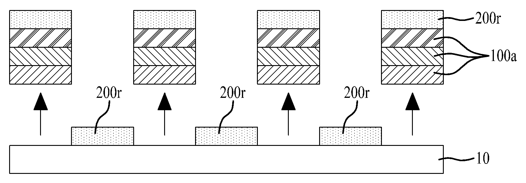
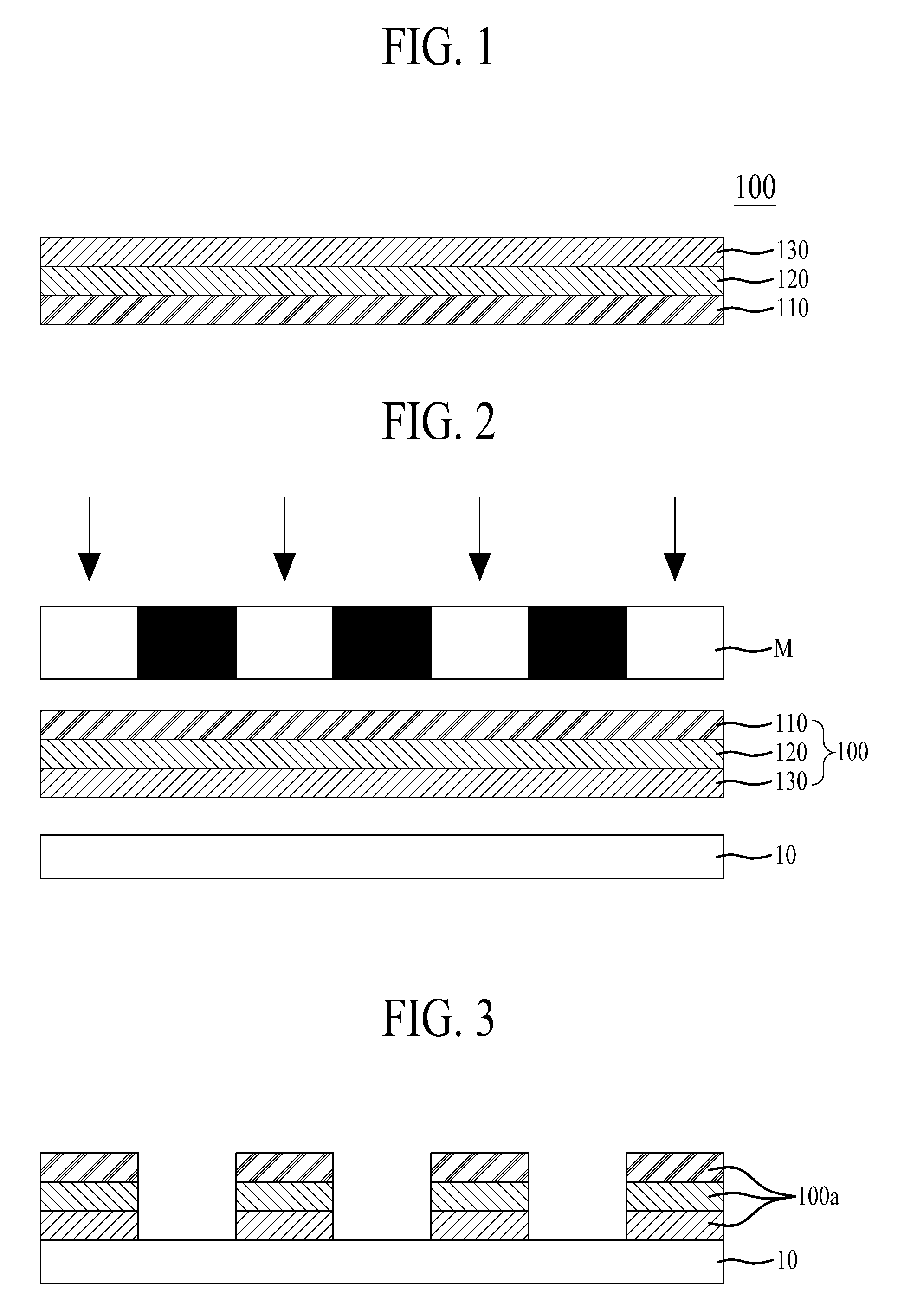
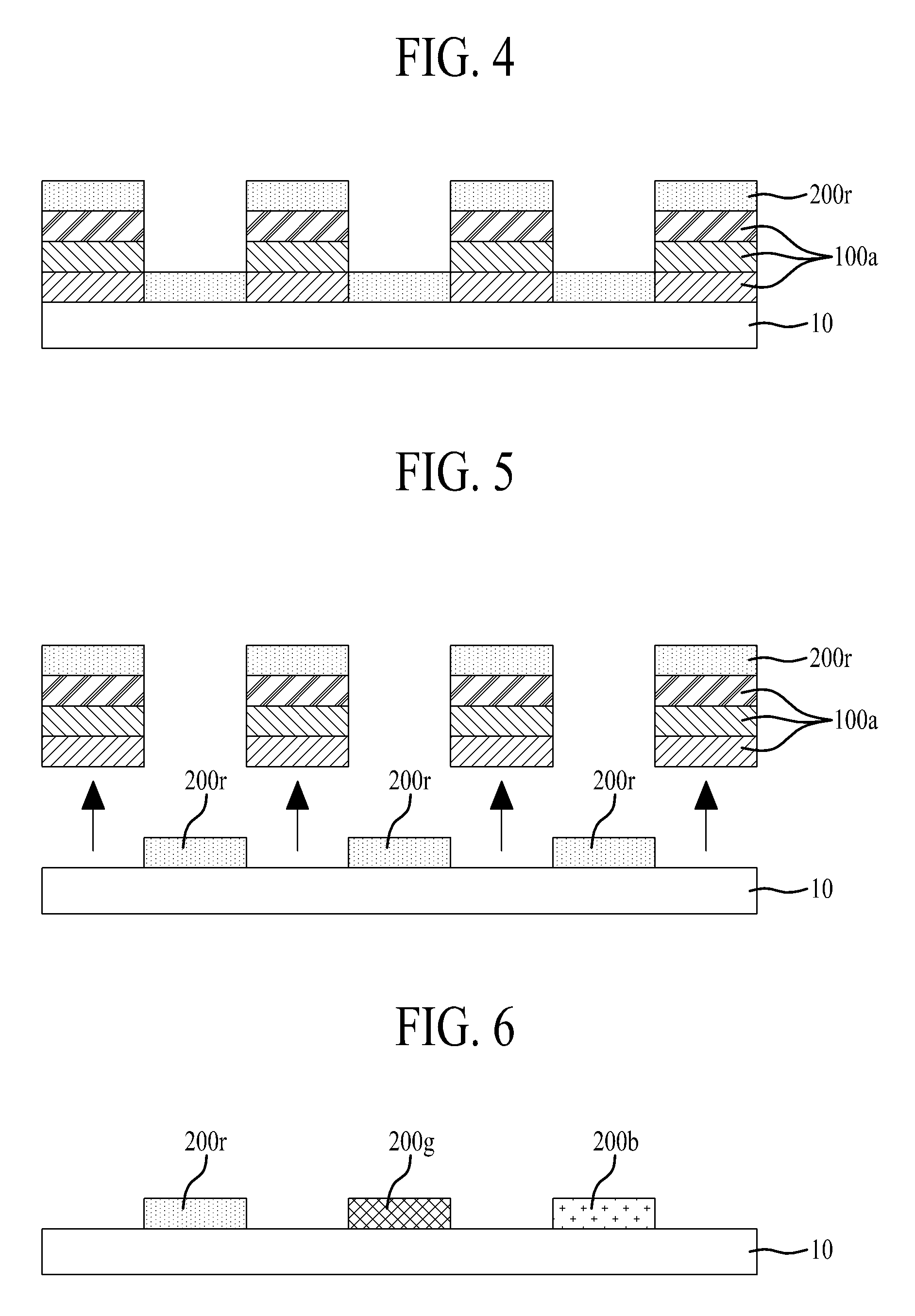

Image

  • Photoresist film and manufacturing method for organic light emitting display device using the same
  • Photoresist film and manufacturing method for organic light emitting display device using the same
  • Photoresist film and manufacturing method for organic light emitting display device using the same

Examples


example 1

[0048]A photoresist film coated with F127 (EO100P065EO100) was formed on a transfer substrate, and then detachment rate and retention rate of emitting layer (EML) for the photoresist film were evaluated.

[0049]At this time, the photoresist film was coated with F127 of thermo-responsive polymer through the use of bar coater method, and a thickness of PEO-PPO-PEO (F127) coated onto the photoresist film was 6 μm.

[0050]After depositing the emitting layer (EML), a temperature was maintained at 120° C. for 5 minutes, and then the photoresist film was removed to evaluate the detachment rate and the retention rate of emitting layer (EML).

[0051]According to the evaluation results, the detachment rate was 58%, and the retention rate of emitting layer (EML) was 65%, wherein the detachment rate and retention rate of emitting layer (EML) were calculated by the same method mentioned in the comparative example.

example 2

[0052]A photoresist film coated with F127 (EO100P065EO100) was formed on a transfer substrate, and then detachment rate and retention rate of emitting layer (EML) for the photoresist film were evaluated.

[0053]At this time, the photoresist film was coated with F127 of thermo-responsive polymer through the use of bar coater method, and a thickness of PEO-PPO-PEO (F127) coated onto the photoresist film was 16 μm.

[0054]After depositing the emitting layer (EML), a temperature was maintained at 120° C. for 5 minutes, and then the photoresist film was removed to evaluate the detachment rate and the retention rate of emitting layer (EML).

[0055]According to the evaluation results, the detachment rate was 72%, and the retention rate of emitting layer (EML) was 83%, wherein the detachment rate and retention rate of emitting layer (EML) were calculated by the same method mentioned in the comparative example.

[0056]As shown in the following Table 1, the detachment rate and retention rate of emitt...


PUM

PropertyMeasurementUnit
LCSTaaaaaaaaaa
LCSTaaaaaaaaaa
temperaturesaaaaaaaaaa

Abstract

Disclosed is a photoresist film including a light-to-heat conversion layer on a support film, and a thermo-responsive polymer layer on the light-to-heat conversion layer, wherein the photoresist film is easily detached from a transfer substrate through a temperature adjustment and detach film since the photoresist film includes thermo-responsive polymer.

Description

CROSS-REFERENCE TO RELATED APPLICATIONS[0001]This application claims the benefit of the Korean Patent Application No. 10-2012-0093762 filed on Aug. 27, 2012, which is hereby incorporated by reference in its entirety.BACKGROUND[0002]1. Field of the Invention[0003]The present invention relates to a photoresist film, and more particularly, a photoresist film and a manufacturing method for an organic light emitting display device using the same.[0004]2. Discussion of the Related Art[0005]An organic light emitting display (OLED) device is one of new flat display devices, and the OLED device can emit light in itself. In comparison with a liquid crystal display (LCD) device, the OLED device has a wider viewing angle and a greater contrast ratio. Furthermore, the OLED device does not require an additional backlight unit, whereby the OLED device can realize thin profile and light weight. Also, the OLED device is advantageous in power consumption. In addition, the OLED device has rapid respon...

Claims


Application Information

Patent Timeline
Patent Type & Authority Patents(United States)
IPC IPC(8): H01L21/00B41M5/46H01L51/56H01L51/00H10K99/00
CPCG03F7/094B41M5/46H01L51/0013H01L51/56B41M2205/06B41M2205/38Y02E10/549Y02P70/50H10K71/18H10K71/00H10K71/16G03F7/004G03F7/0045G03F7/09G03F7/11H05B33/10
Inventor PARK, JAE HYUNKIM, JIN WUKKIM, WY-YONGMIN, HYE LIKIM, MIN JEESON, YOUNG TAESHIN, YOUNG SUB
Owner LG DISPLAY CO LTD
Learn More