Field-effect transistor comprising a leakage-current limiter

a field-effect transistor and limiter technology, applied in the field of organic field-effect transistors, can solve the problems of modifying the other transistor, using this type of organic field-effect transistor to form electric circuits, and increasing the manufacturing cost of such transistors, so as to reduce the manufacturing cost, and reduce the manufacturing cos

Inactive Publication Date: 2015-08-18
COMMISSARIAT A LENERGIE ATOMIQUE ET AUX ENERGIES ALTERNATIVES
View PDF14 Cites 0 Cited by
  • Summary
  • Abstract
  • Description
  • Claims
  • Application Information

AI Technical Summary

Benefits of technology

[0013]One of the aims of the invention thus is to overcome such disadvantages by providing a field-effect transistor of simple design, low cost, and limiting the leakage current between the gate electrode and the source or drain electrode without modifying the intrinsic characteristics of the dielectric layer.

Problems solved by technology

Such a degradation of current Ioff of the field-effect transistor, due to the leakage current appearing between the gate electrode and the source electrode in the dielectric layer, forbids the use this type of organic field-effect transistor to form electric circuits.
However, modifying the intrinsic properties of dielectric layer 6 or increasing its thickness increases the manufacturing costs of such transistors and also modifies the other transistor characteristics, such as, particularly, the capacitance of the dielectric layer, which is then capable of generating stray capacitances also altering the proper operation of the transistor.

Method used


Image

  • Field-effect transistor comprising a leakage-current limiter
  • Field-effect transistor comprising a leakage-current limiter
  • Field-effect transistor comprising a leakage-current limiter

Examples


example of embodiment

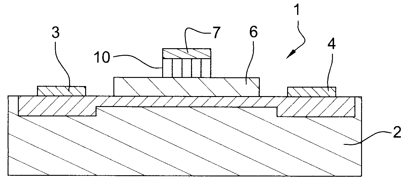
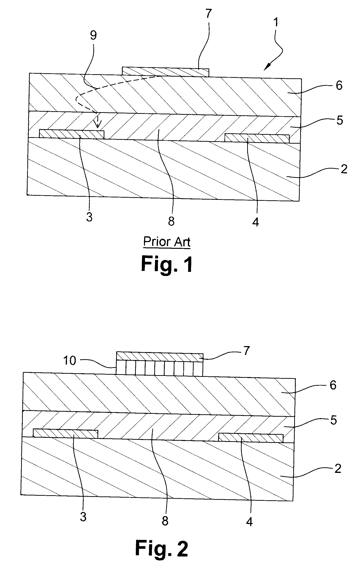
[0050]Referring to FIG. 7, field-effect transistor 1 is obtained by deposition on a substrate of polyethylene naphthalate (PEN) having an approximate thickness of 125 micrometers, forming lower substrate 2 of the transistor, and of 3 nanometers of gold (Au).

[0051]The gold layer (Au) is then etched to obtain a source electrode 3 and a drain electrode 4.

[0052]A semiconductor layer 5 made of triisopropylsilyl pentacene (TIPS) having an approximate thickness of 90 nanometers is then deposited by photogravure, and covered with a dielectric fluoropolymer layer 6, sold under trade name CYTOP® for example, having an approximate thickness of 800 nanometers.

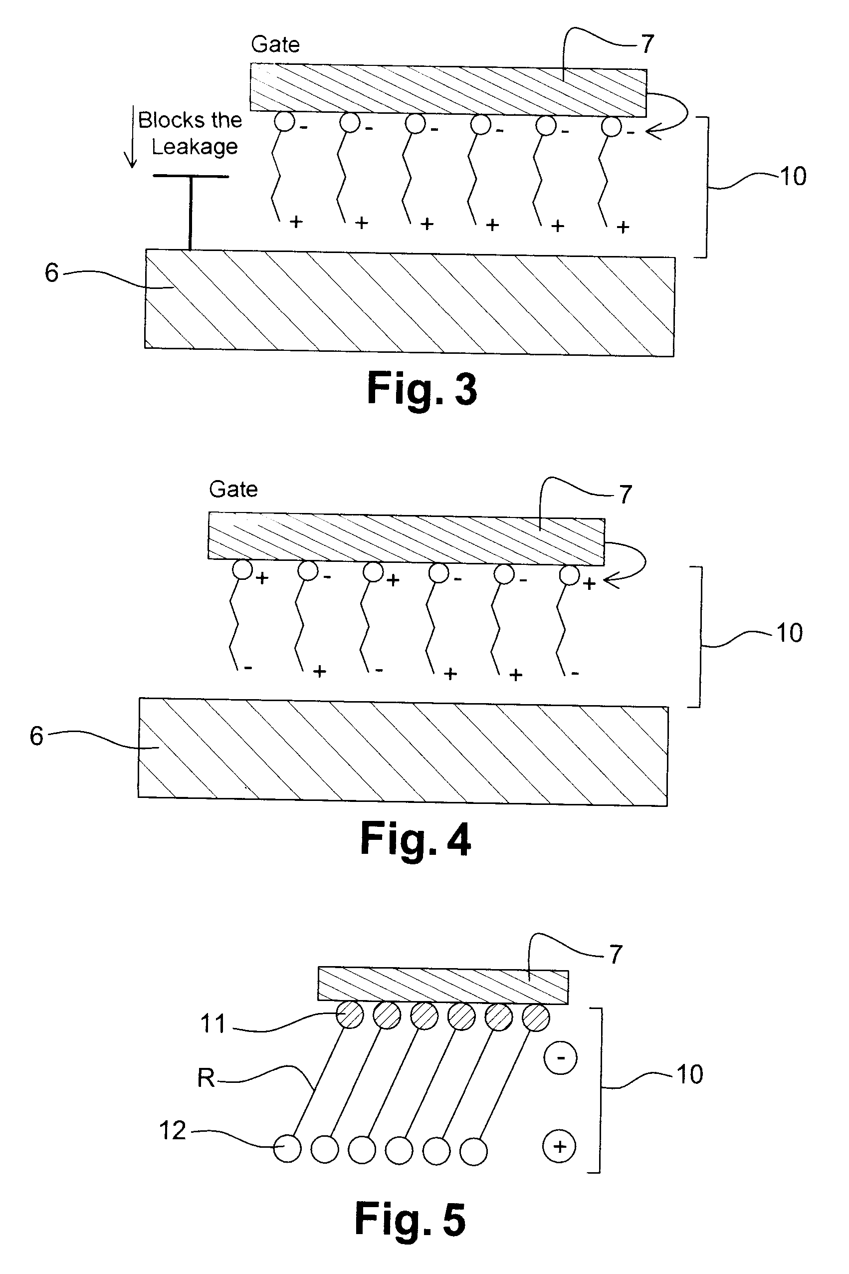
[0053]Then, cysteine molecules of general formula HSNH2COOH are deposited by inkjet on a portion of the upper surface of dielectric layer 6 at the level of gate electrode 7 to form an intermediate layer 10.

[0054]Finally, 50 nanometers of gold are deposited on said intermediate layer 10 to form gate electrode 7.

[0055]Intermediate layer 10 m...


PUM


Abstract

A field-effect transistor including at least one lower substrate having two electrodes deposited thereon, respectively a source electrode and a drain electrode, a dielectric layer made of a dielectric material, and a gate electrode deposited on the dielectric layer. It includes an intermediate layer, made of a material comprising molecules having a dipole moment complying with specific direction criteria, deposited between the gate electrode and the dielectric layer, said intermediate layer extending at least under the entire surface area taken up by the gate electrode, the intermediate layer being made of an organic compound comprising at least one binding function for the gate electrode.

Description

FIELD OF THE INVENTION[0001]The present invention relates to the field of organic transistors, such as, for example, organic thin-film transistors (OTFT). It more specifically relates to an organic transistor comprising means enabling to limit leakage currents appearing between the gate and the semiconductor of said transistor.BACKGROUND[0002]FIG. 1 shows an organic thin-film transistor of prior art, having a so-called “high-gate” and “low-contact” structure. In this instance, said transistor 1 comprises:[0003]a lower substrate 2, having two electrodes 3, 4, a first source electrode 3 and a second drain electrode 4, formed thereon,[0004]a semiconductor layer 5 made of a semiconductor material and deposited on lower substrate 2, source electrode 3 and drain electrodes 4,[0005]and a dielectric layer 6 made of a dielectric material and deposited on semiconductor layer 5, and having a gate electrode 7 formed thereon.[0006]The transistor effect is obtained, as known per se, by applying a...

Claims


Application Information

Patent Timeline
Patent Type & Authority Patents(United States)
IPC IPC(8): H01L29/08H01L51/00H01L51/05
CPCH01L51/0529H01L51/0001H01L51/0541H10K10/474H10K10/464H10K71/00
Inventor BENWADIH, MOHAMMED
Owner COMMISSARIAT A LENERGIE ATOMIQUE ET AUX ENERGIES ALTERNATIVES
Why Eureka
Try Eureka