

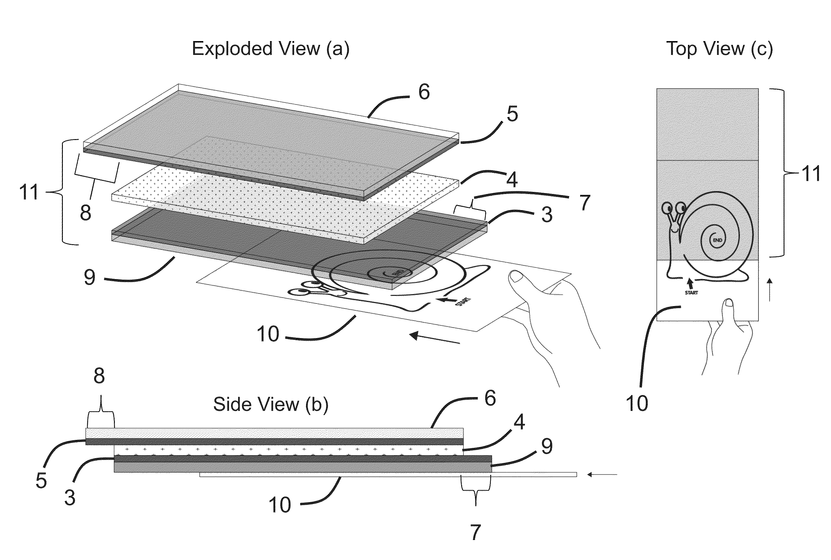
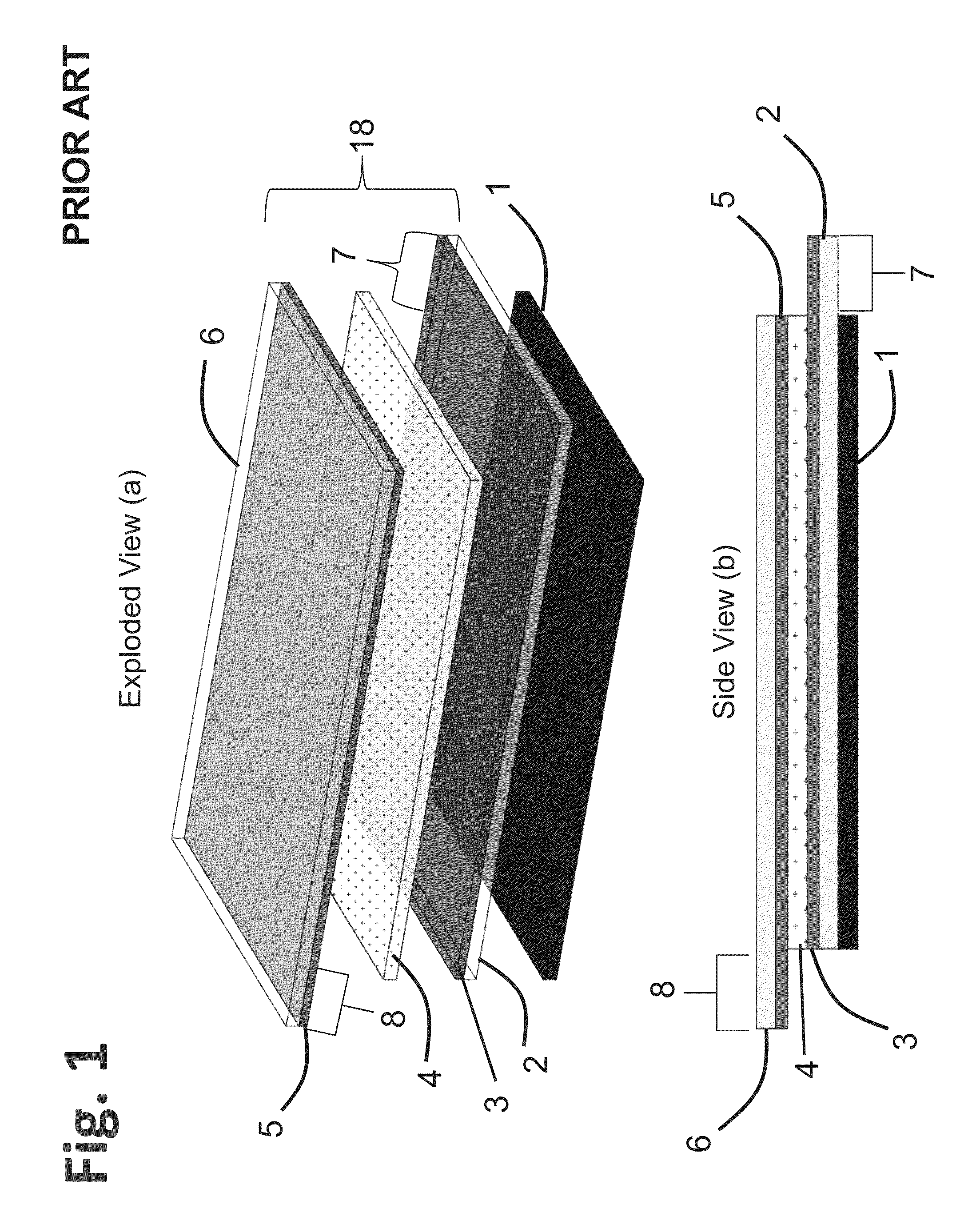
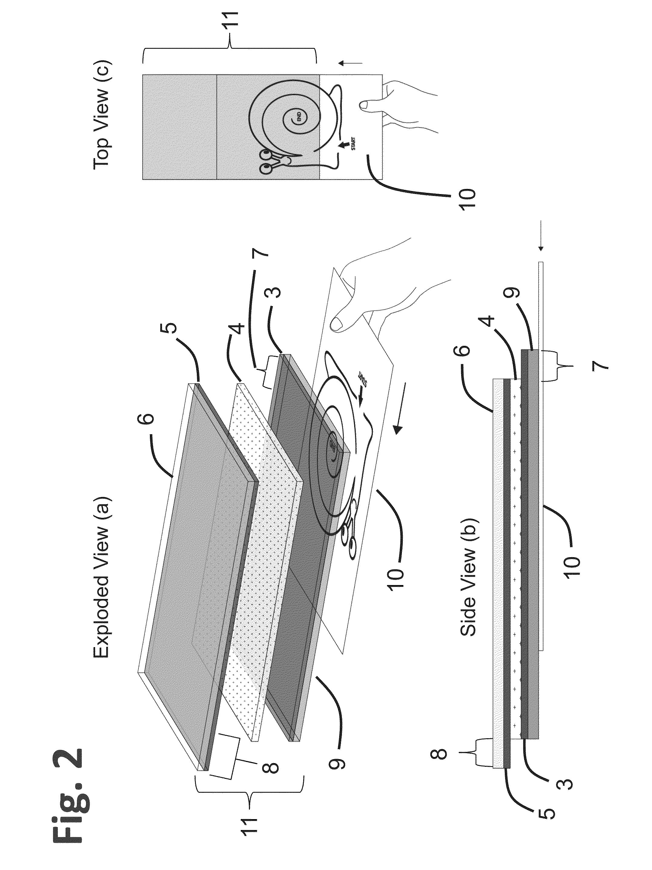
Electronic display with semitransparent back layer
a technology of semi-transparent back layer and electronic display, applied in the field of electronic display, can solve the problems of fixed background color and any background pattern on the tablet, and achieve the effect of reducing gap regions and reducing gaps
- Summary
- Abstract
- Description
- Claims
- Application Information
AI Technical Summary
Benefits of technology
Problems solved by technology
Method used
Image

Examples
example 1
[0063]A Boogie Board™ writing tablet purchased from a Brookstone retail store was disassembled so that the opaque coating from the back substrate could be removed. The removal of the ink was done using a methanol wipe. After cleaning, the display was coated with Norcote brand blue process ink. Once the ink was dried, the display and electronics were assembled on a thin sheet of clear acrylic. The result of this process changes the display from a writer with yellow writing on a black background to one with yellow writing on a semitransparent blue background. A photograph of the result is shown in FIG. 5.
example 2
[0064]In FIG. 9, the reflection spectra of a solid yellow template is shown by the solid line. When a writing tablet with blue semitransparent backcoat, operating in the B mode, is placed on the template, the region with no writing (focal conic or dark state) has a reflection spectra shown by the dotted line. This resultant spectra is due to color subtraction of the yellow template spectra by the blue semitransparent coating that cut off most of the reflected light beyond 500 nm and also absorption of some of the light by the template in wavelengths less than 450 nm. The written region would show a reflection spectra shown by the dashed line, which includes the result of color subtraction of the yellow template and blue coating in cooperation with color addition due to the liquid crystal layer reflecting light between 485-640 nm.
example 3
[0065]In FIG. 10, the reflection spectra of a solid white template is shown by the solid line. When a writing tablet with blue semitransparent backcoat, operating in the B mode, is placed on the template, the region with no writing (focal conic) has a reflection spectra shown by the dotted line. This resultant spectra is due to color subtraction of the white spectra by the blue semitransparent coating that cut off most of the reflected light beyond 550 nm and lets about 30% of the light at around 475 nm. The written region would show a reflection spectra shown by the dashed line, which includes the result of color subtraction from the blue coating in cooperation with color addition due to the liquid crystal layer reflecting light between 485-640 nm.
[0066]FIG. 11 shows an article generally represented by 600 including electronic skin liquid crystal display 11 of this disclosure. the article 600 is selected from the group consisting of cellphone, laptop, computer, computer monitor, co...
PUM
| Property | Measurement | Unit |
|---|---|---|
| transparency | aaaaa | aaaaa |
| thickness | aaaaa | aaaaa |
| wavelengths | aaaaa | aaaaa |
Abstract
Description
Claims
Application Information