Display panel

a display panel and panel technology, applied in the field of panels, can solve the problems of non-conformity between the pattern locations formed, affecting the display quality of the display panel, and non-conformity to the properties, and achieve the effect of improving the poor display quality

Active Publication Date: 2015-09-01
AU OPTRONICS CORP
View PDF24 Cites 4 Cited by
  • Summary
  • Abstract
  • Description
  • Claims
  • Application Information

AI Technical Summary

Benefits of technology

[0007]Accordingly, the invention is directed to a display panel, which may improve the poor display quality generated by the parasitic capacitance variation that is caused by the displacement offset.
[0025]Based on the above descriptions, in the display panel of the invention, the first terminal and the second terminal (constituted by the same film) of the first control transistor are sequentially arranged on the forward direction of the first direction, and the first terminal and the second terminal (constituted by the same film) of the second control transistor are sequentially arranged on the reverse direction of the first direction. In this way, when the position of a photomask for forming the first and second terminals of the transistors occurs an offset on the first direction during a manufacturing process, the deviated locations of the first terminal and the second terminal of the first control transistor in relative to the location of the third terminal of the first control transistor may compensate the deviated locations of the first terminal and the second terminal of the second control transistor in relative to the location of the third terminal of the second control transistor. Therefore, the parasitic capacitance variations are generated in the two control transistors (that is due to the photomask offset in the manufacturing process), where the parasitic capacitance variation of one control transistor is increased and the parasitic capacitance variation of another control transistor is decreased, thereby compensating with each other. In the embodiments of the invention, the control circuit for driving the light emitting units with the same color concurrently includes the two aforementioned control transistors, and the display panel may still have the uniform display quality, even if the photomask occurs a location offset during the manufacturing process.

Problems solved by technology

The existence of these parasitic capacitances may affect the element properties of the thin film transistor structure, thereby affecting the display quality of the display panel.
Therefore, in the exposure process, the displacement offsets resulting from movements of the machine would cause nonconformity among the pattern locations formed in each exposure shot.
At this moment, the thin film transistors in the different exposure shots may have different parasitic capacitances Cgs and Cgd, thereby causing nonconformity to the properties of thin film transistor, and thus the uneven brightness issue on the whole display panel is occurred during displaying.

Method used


Image

  • Display panel
  • Display panel
  • Display panel

Examples


first embodiment

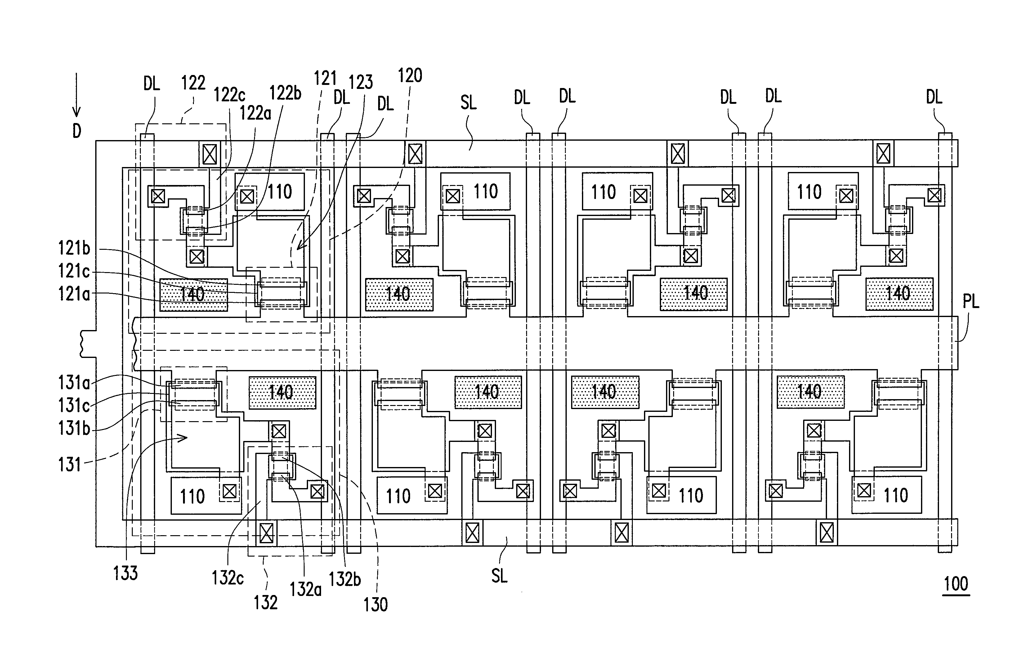
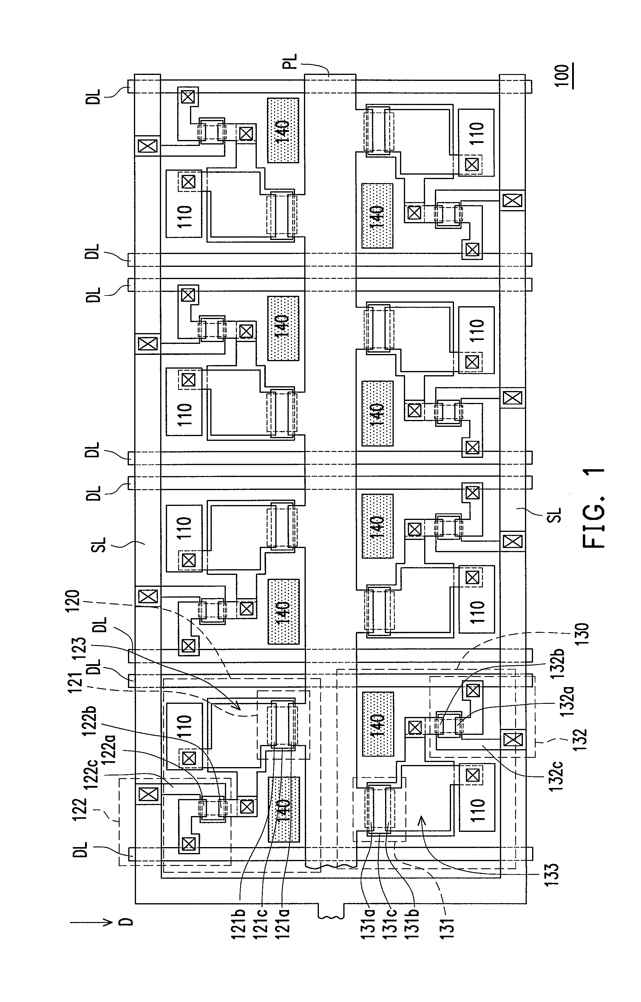
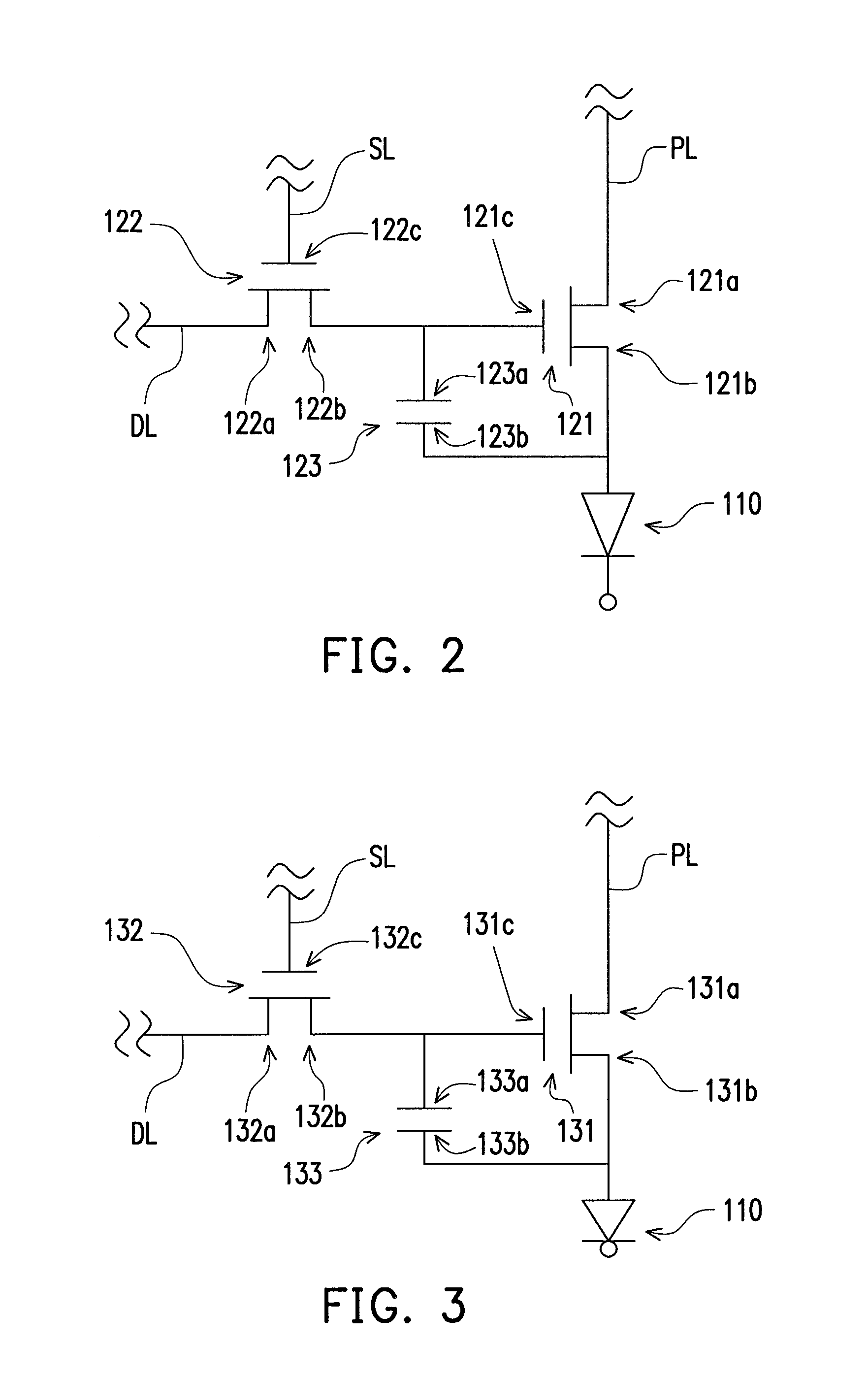
[0042]FIG. 1 is a schematic top view illustrating a display panel according to the invention. Referring to FIG. 1, the display panel 100 includes a plurality of scan lines SL, a plurality of data lines DL, a plurality of power lines PL, a plurality of light emitting units 110, a plurality of first pixel circuits 120 and a plurality of second pixel circuits 130. The light emitting units 110 are arranged in an array. The first pixel circuits 120 are connected to the corresponding scan lines SL, data lines DL and power lines PL, furthermore, some parts of the light emitting units 110 are connected to the first pixel circuits 120. The second pixel circuits 130 are connected to the corresponding scan lines SL, data lines DL and power lines PL, furthermore, the rest of the light emitting units 110 are connected to the second pixel circuits 130.

[0043]The display panel 100 is substantially employed with two kinds of pixel circuit 120 and 130 to drive the light emitting units 110. Furthermor...

second embodiment

[0073]Similarly, in the second embodiment, the organic light emitting units 210 with the same color are designed as that some parts are connected to the first pixel circuits 220, while other parts are connected to the second pixel circuits 230. As described in the aforementioned embodiment, the arrangements of the first terminal 222a and the second terminal 222b of the first control transistor 222 and the first terminal 232a and the second terminal 232b of the second control transistor 232 on the first direction D2 are incorporated to compensate the parasitic capacitance variation caused by the displacement offset of photomasks in the fabrication.

[0074]In addition, a repeat unit B is formed by taking eight light emitting units 210 from the light emitting units 210 in the display panel 200 as a group, and the repeat units B are repeatedly arranged. Furthermore, a repeat unit B is constituted by arranging the two same sub units B1 side by side, wherein the color combination and the ar...

fourth embodiment

[0080]In the fourth embodiment, the light emitting units 410 on the same row are arranged in this order of red, blue and green repeatedly. The arrangement illustrated in FIG. 9 is exemplified, where the light emitting units 410 on the first row are arranged in the order of red, blue and green, the light emitting units 410 on the second row are also arranged in the same order of red, blue and green, and the light emitting units 410 on the same column can have the same color. This means that all the light emitting units 410 on the first column are the red light emitting units 410a, all the light emitting units 410 on the second column are the green light emitting units 410b, and all the light emitting units 410 on the third column are the white light emitting units 410c. Similarly, the light emitting units 410 on the fourth column are the red light emitting units 410a, the light emitting units 410 on the fifth column are the green light emitting units 410b and the light emitting units...


PUM


Abstract

A display panel includes a plurality of scan lines, a plurality of data lines, a plurality of power lines, a plurality of light emitting units, a plurality of first pixel circuits and a plurality of second pixel circuits. The plurality of light emitting units are arranged in an array and adapted to display different colors. In the organic light emitting units with the same color, some parts are connected to the first pixel circuits, and other parts are connected to the second pixel circuits. A first terminal and a second terminal of a first control transistor in the first pixel circuit are sequentially arranged on a forward direction of a first direction, and a first terminal and a second terminal of a second control transistor in the second pixel circuit are sequentially arranged on a reverse direction of the first direction.

Description

CROSS-REFERENCE TO RELATED APPLICATION[0001]This application claims the priority benefit of Taiwan application serial no. 101128840, filed on Aug. 9, 2012, the entirety of the above-mentioned patent application is hereby incorporated by reference herein and made a part of this specification.BACKGROUND[0002]1. Technical Field[0003]The invention relates to a panel, and more particularly, to a display panel.[0004]2. Related Art[0005]Thin film transistors are often utilized as a switching element of a pixel structure in a display panel. In the known thin film transistor structure, a gate and a source of the thin film transistor structure are constituted of different films, and are overlapped with each other in certain region, therefore, a gate-source parasitic capacitance Cgs exists between the two electrodes. Similarly, a gate and a drain of the thin film transistor structure are constituted of different films, and are also overlapped with each other in certain region, therefore, a gat...

Claims


Application Information

Patent Timeline
Patent Type & Authority Patents(United States)
IPC IPC(8): H01L27/32G09G3/32H01L29/417
CPCH01L27/3276H01L27/326G09G3/3233H01L29/41733H10K59/121H10K59/131
Inventor XI, PENG-BOCHANG, LEE-HSUNLIN, LI-FONG
Owner AU OPTRONICS CORP
Why Eureka
Try Eureka