

Heterojunction bipolar transistor, power amplifier including the same, and method for fabricating heterojunction bipolar transistor
a technology of heterojunction bipolar transistor and power amplifier, which is applied in the direction of transistors, semiconductor devices, electrical devices, etc., can solve the problems of deterioration of power amplifier characteristics, affecting the performance of power amplifiers, and the unit hbt connected in parallel does not operate uniformly, so as to achieve the effect of improving power amplifier characteristics
- Summary
- Abstract
- Description
- Claims
- Application Information
AI Technical Summary
Benefits of technology
Problems solved by technology
Method used
Image

Examples
first preferred embodiment
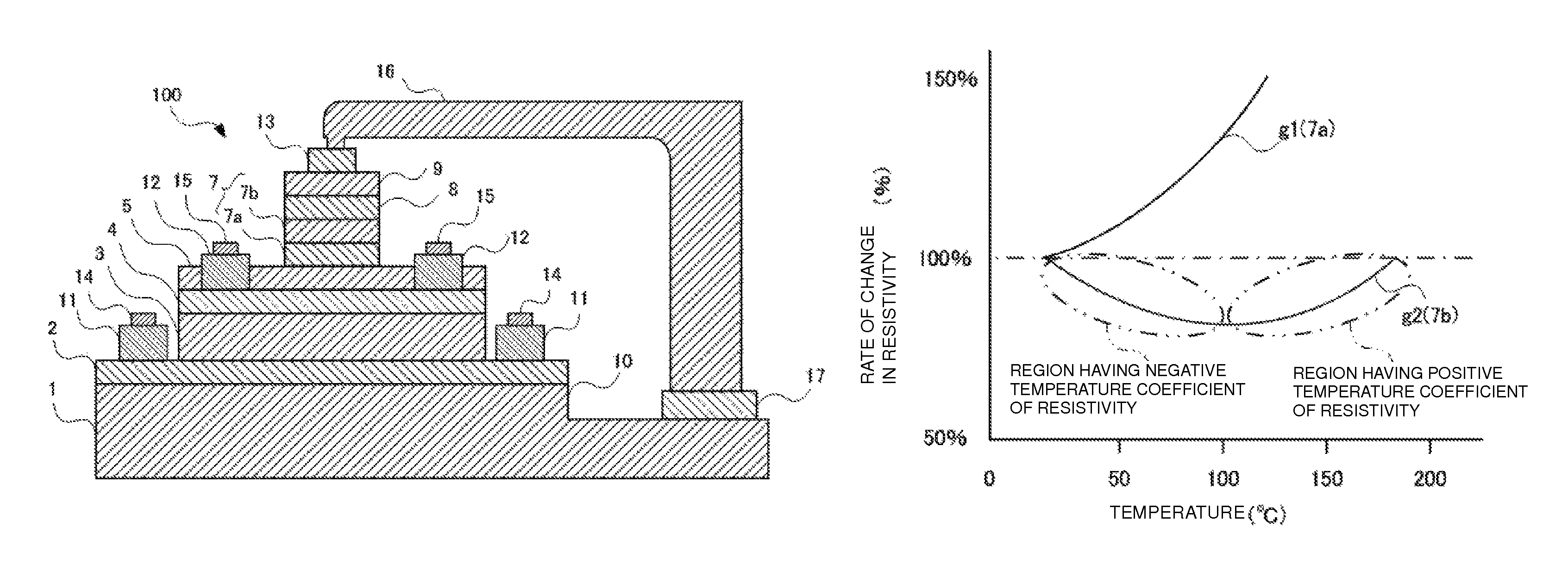
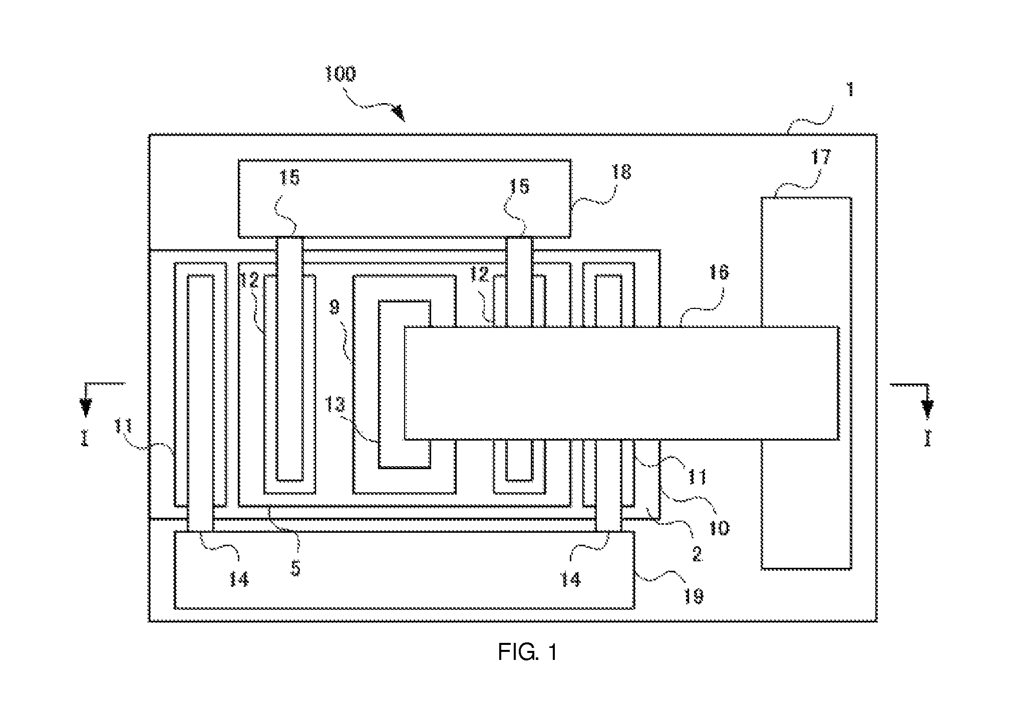
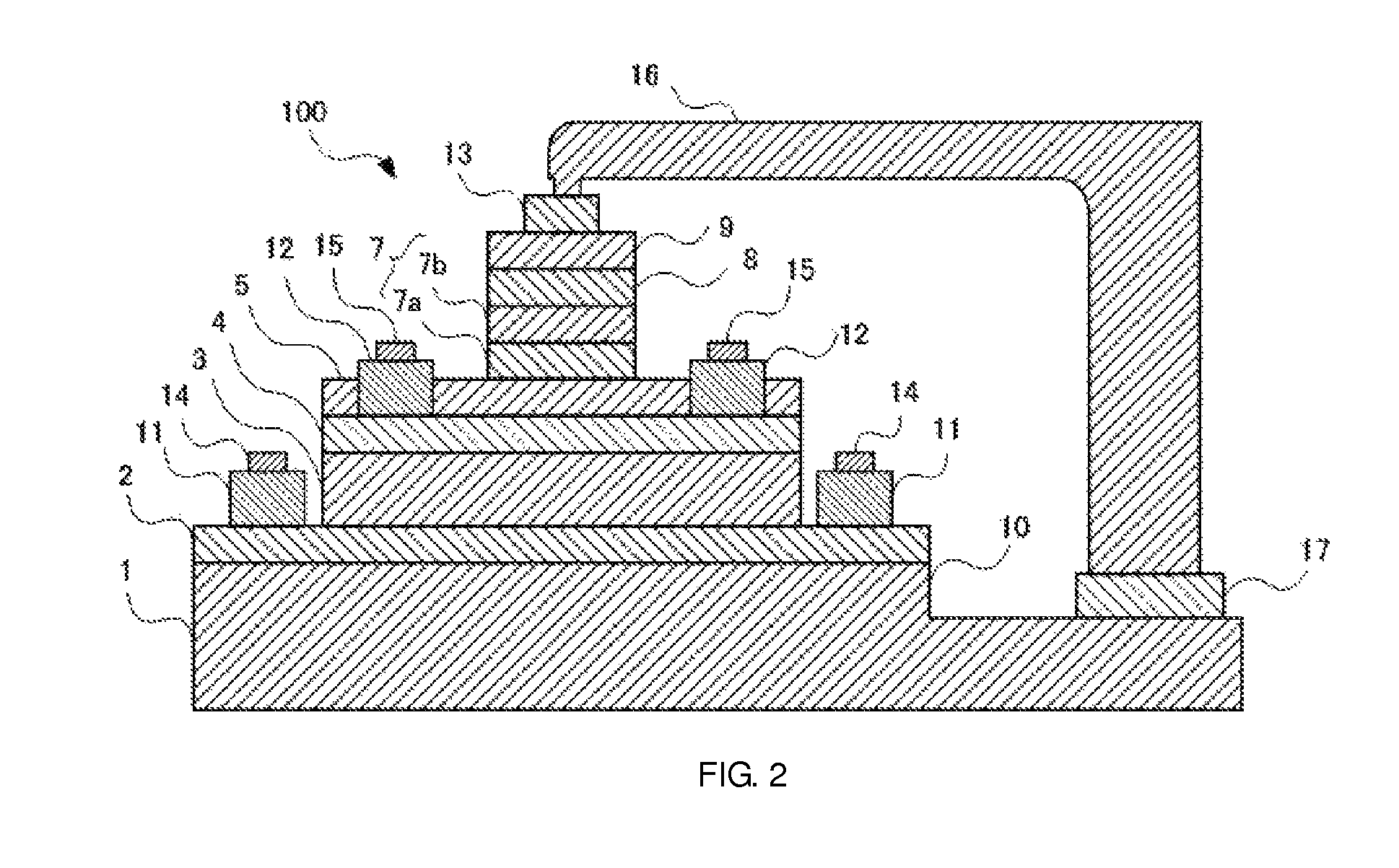
[0036]FIG. 1 is a plan view of an HBT 100 (a rectangular or substantially rectangular emitter with a size of about 3 μm×about 20 μm, for example) according to a first preferred embodiment of the present invention. FIG. 2 is a sectional view taken along the line I-I of FIG. 1. As illustrated in FIGS. 1 and 2, an n-type GaAs sub-collector layer 2 having a Si concentration of about 5×1018 cm−3 and a film thickness of about 0.6 μm is placed on a semi-insulating GaAs substrate 1. The following layers are arranged on the n-type GaAs sub-collector layer 2 in this order: an n-type GaAs collector layer 3 having a Si concentration of about 1×1016 cm−3 and a film thickness of about 1.0 μm; a p-type GaAs base layer 4 having a C concentration of about 4×1019 cm−3 and a film thickness of about 150 nm; and an n-type InGaP emitter layer 5 having an In-to-P molar ratio of 0.5, a Si concentration of about 3×1017 cm−3, and a film thickness of about 30 nm. Base electrodes 12 are arranged in the n-type ...
second preferred embodiment
[0048]A second preferred embodiment of the present invention will now be described. The second preferred embodiment is different from the first preferred embodiment in that the configuration of a ballast resistor layer 7 is varied. The same components as those described in the first preferred embodiment are designated by the same reference numerals as those used in the first preferred embodiment and will not be described in detail.
[0049]FIG. 5 is a sectional view of an HBT 100, according to the second preferred embodiment, taken along the line I-I. FIG. 5 is different from FIG. 2 in the configuration of the ballast resistor layer 7. In particular, in the second preferred embodiment, the ballast resistor layer 7 includes an n-type AlGaAs emitter ballast resistor sub-layer 7c which is a first ballast resistor sub-layer and which has an Al-to-As molar ratio of about 0.33, a Si concentration of about 5.4×1016 cm−3, and a film thickness of about 26 nm and an n-type AlGaAs emitter ballast...
third preferred embodiment
[0059]A third preferred embodiment of the present invention will now be described. The third preferred embodiment is different from the first preferred embodiment in that the configuration of a ballast resistor layer 7 is varied. The same components as those described in the first preferred embodiment are designated by the same reference numerals as those used in the first preferred embodiment and will not be described in detail.
[0060]FIG. 8 is a sectional view of an HBT 100, according to the third preferred embodiment, taken along the line I-I. FIG. 8 is different from FIG. 2 in that the configuration of a ballast resistor layer 7. In particular, in the third preferred embodiment, the ballast resistor layer 7 preferably includes three sub-layers: an n-type AlGaAs emitter ballast resistor sub-layer 7e which is a third ballast resistor sub-layer and which has an Al-to-As molar ratio of about 0.33, a Si concentration of about 5.0×1017 cm−3, and a film thickness of about 61 nm; an n-ty...
PUM
 Abstract
Description
Claims
Application Information