High speed bypass cable for use with backplanes

a bypass cable and backplane technology, applied in the direction of connection, electrical apparatus, coupling device connection, etc., can solve the problems of severely increasing the cost of the circuit board, and undesirable use of fr-4 materials, and achieve the effect of low loss characteristics

Active Publication Date: 2015-09-22
MOLEX INC
View PDF15 Cites 61 Cited by
  • Summary
  • Abstract
  • Description
  • Claims
  • Application Information

AI Technical Summary

Benefits of technology

[0006]Accordingly, there is provided an improved high speed bypass cable assembly that defines a signal transmission line useful for high speed applications at 10 GBps or above and with low loss characteristics.
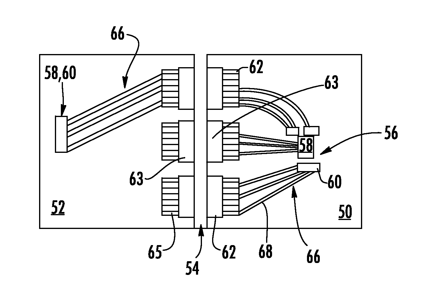
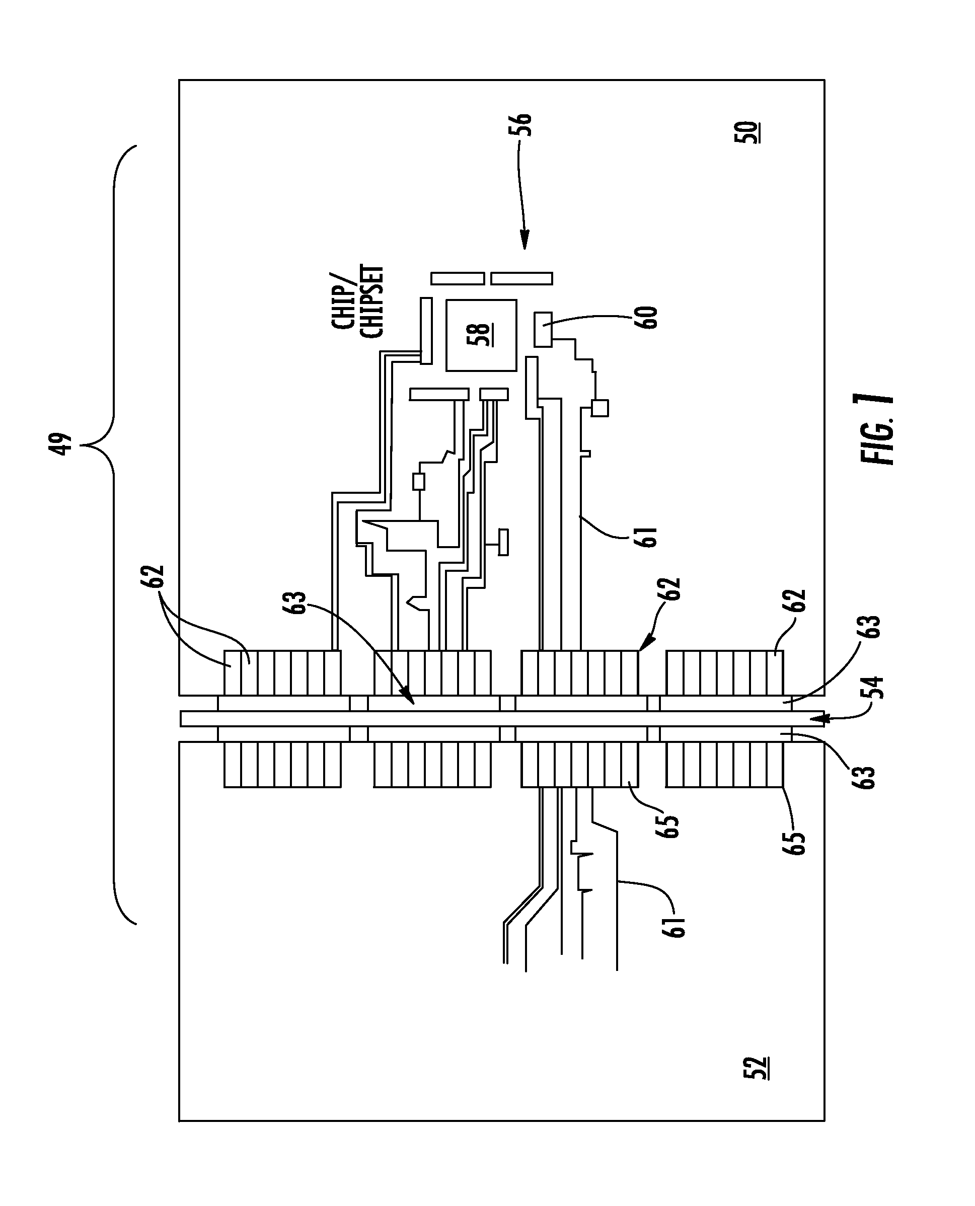
[0007]In accordance with an embodiment described in the Present Disclosure, an electrical cable assembly can be used to define a high speed transmission line extending between an electronic component, such as a chip, or chip set, and a predetermined location on a backplane. Inasmuch as the chip is typically located a long length from the aforesaid location, the cable assembly acts a signal transmission line that that avoids, or bypasses, the landscape of the circuit board construction and which provides an independent signal path line that has a consistent geometry and structure that resists signal loss and maintains its impedance at a consistent level without great discontinuity.
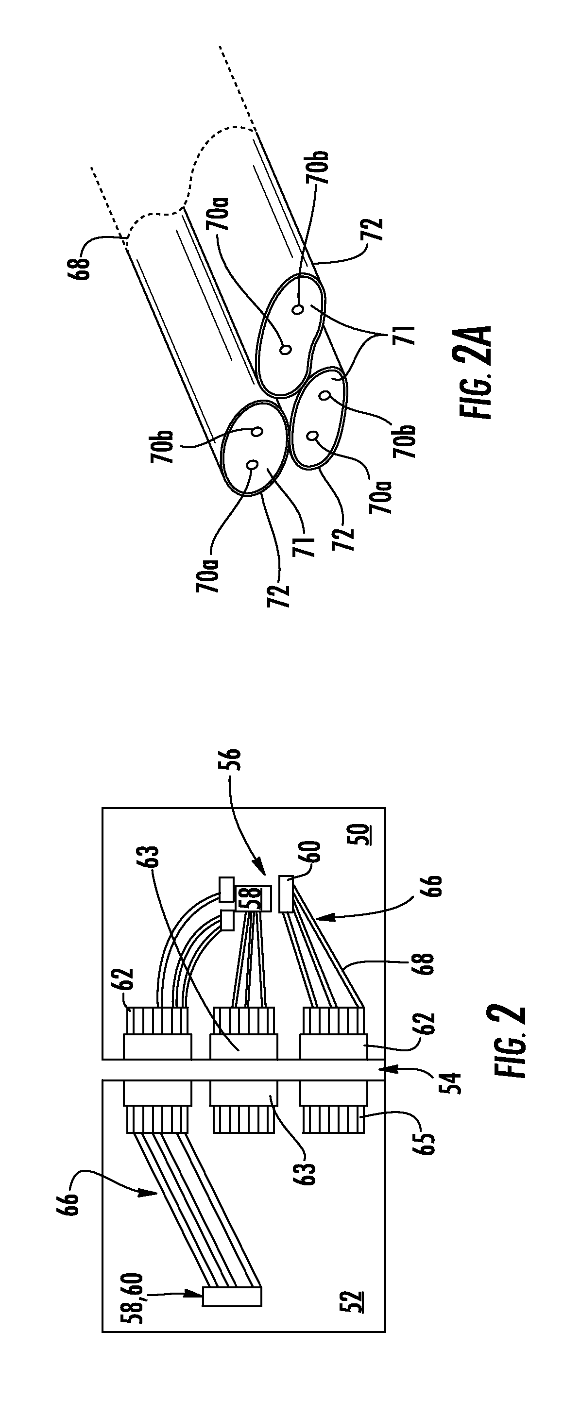
[0008]In accordance with the Present Disclosure, the cable may include one or more cables which contain dedicated signal transmission lines in the form of pairs of wires that are enclosed within an outer, insulative covering and which are known in the art as “twin-ax” wires. The spacing and orientation of the wires that make up each such twin-ax pair can be easily controlled in a manner such that the cable assembly provides a transmission line separate and apart from the circuit board, and which extends between a chip or chip set and a connector location on the circuit board. Preferably, a backplane style connector is provided, such as a pin header or the like, which defines a transition that does not inhibit the signal transmission. The cable twin-ax wires are terminated directly to the termination tails of a mating connector so that crosstalk and other deleterious factors are kept to a minimum at the connector location.
[0010]The cable wires are preferably terminated to blade-style terminals in each connector wafer, which mate with opposing blade portions of corresponding terminals of a pin header. The pin header penetrates through the intervening circuit board and the pins of the header likewise mate with like cable connectors on the other side of the circuit board. In this manner, multiple bypass cable assemblies may be used as signal transmission paths. This structure eliminates the need for through-hole or compliant pin connectors as well as avoids the need for long and possibly complex routing paths in the circuit board. As such, a designer may use inexpensive FR4 material for the circuit board construction, but still obtain high speed performance without degrading losses.
[0012]In one embodiment, grounding cradles are provided for each twin-ax wire pair so that the grounding shield for each twin-ax wire may be terminated to the two corresponding grounding terminals that flank the pair of the interior signal terminals. In this manner, the geometry and spacing of the cable signal wires is maintained to the extent possible through the connector termination area. The connector terminals are configured to minimize the impedance discontinuity occurring through the connector so that designed impedance tolerances may be maintained through the connector system.
[0015]The cable clamps may be crimped to the outer shielding members of each twin-ax cable and the cable clamps, the ground strip, free ends of the twin-ax cables and free ends of the connector terminals are disposed in a termination area of the wafer connector. This area is overmolded with a dielectric material that forms a solid mass that is joined to the connector frame. The ground strip commons the outer shielding members of the twin-ax wires together, as well as the ground terminals of the connector to provide a reliable ground path.

Problems solved by technology

However, FR-4 is known to promote losses in high speed signal transmission lines, and these losses make it undesirable to utilize FR-4 material for high speed applications of about 10 Gbps and greater.
Custom materials for circuit boards are available that reduce such losses, but the prices of these materials severely increase the cost of the circuit board and, consequently, the electronic devices in which they are used.
These long lengths require that the signals traveling through the transmission line be amplified and repeated, thereby increasing the cost of the circuit board, and complicating the design inasmuch as additional board space is needed to accommodate these amplifiers and repeaters.
In addition, the routing of the traces of such a transmission line in the FR-4 material may require multiple turns.
It then becomes difficult to route transmission line traces in a manner to achieve a consistent impedance and a low signal loss therethough.
It therefore becomes difficult to adequately design signal transmission lines in circuit boards, or backplanes, to meet the crosstalk and loss requirements needed for high speed applications.
It is desirable to use economical board materials such as FR4, but the performance of FR4 falls off dramatically as the data rate approaches 10 Gbps, driving designers to use more expensive board materials and increasing the overall cost of the device in which the circuit board is used.

Method used


Image

  • High speed bypass cable for use with backplanes
  • High speed bypass cable for use with backplanes
  • High speed bypass cable for use with backplanes

Examples


Embodiment Construction

[0058]While the Present Disclosure may be susceptible to embodiment in different forms, there is shown in the Figures, and will be described herein in detail, specific embodiments, with the understanding that the Present Disclosure is to be considered an exemplification of the principles of the Present Disclosure, and is not intended to limit the Present Disclosure to that as illustrated.

[0059]As such, references to a feature or aspect are intended to describe a feature or aspect of an example of the Present Disclosure, not to imply that every embodiment thereof must have the described feature or aspect. Furthermore, it should be noted that the description illustrates a number of features. While certain features have been combined together to illustrate potential system designs, those features may also be used in other combinations not expressly disclosed. Thus, the depicted combinations are not intended to be limiting, unless otherwise noted.

[0060]In the embodiments illustrated in ...


PUM


Abstract

A cable bypass assembly is disclosed for use in providing a high speed transmission line for connecting a chip, processor or circuitry mounted on a circuit board to other similar components. The bypass cable assembly has a structure that maintains the geometry of the cable in place from the chip to the connector and then through the connector. The connector includes a plurality of conductive terminals and shield members arranged within an insulative support frame in a manner that approximates the structure of the cable so that the impedance and other electrical characteristics of the cable may be maintained as best is possible through the cable termination and the connector.

Description

REFERENCE TO RELATED APPLICATIONS[0001]The Present Disclosure is a Continuation-In-Part Application of, and claims priority to, previously-filed U.S. application Ser. No. 13 / 779,027, entitled “High Speed Bypass Cable For Use With Backplanes,” filed on 27 Feb. 2013 with the United States Patent And Trademark Office. Applicants hereby claim priority of the '027 Application under 35 U.S.C. §120. Further, the content of the aforementioned Patent Application is incorporated in its entirety herein.BACKGROUND OF THE PRESENT DISCLOSURE[0002]The Present Disclosure relates, generally, to cable interconnection systems, and, more particularly, to bypass cable interconnection systems for transmitting high speed signals at low losses from chips or processors to backplanes.[0003]Conventional cable interconnection systems are found in electronic devices such as routers, servers and the like, and are used to form signal transmission lines between a primary chip member mounted on a printed circuit bo...

Claims


Application Information

Patent Timeline
Patent Type & Authority Patents(United States)
IPC IPC(8): H01R9/03H01R13/6587H01R13/514H01R13/6471H01R13/6477
CPCH01R13/6471H01R13/514H01R13/6477H01R13/6587Y10S439/941H01R13/6473H01R13/6581H01R12/7076H01R13/6461H01R13/6592H01R13/6474
Inventor WANHA, CHRISTOPHER D.LLOYD, BRIAN KEITHABUNASRAH, EBRAHIMKHAN, REHANRESENDEZ, JAVIERROST, MICHAEL
Owner MOLEX INC
Why Eureka
Try Eureka