Apparatus for probing die electricity and method for forming the same

a technology of apparatus and die, applied in the direction of electronic circuit testing, measurement devices, instruments, etc., can solve the problem of inevitably finding chips with defects

Active Publication Date: 2015-10-13
MPI CORP
View PDF30 Cites 3 Cited by
  • Summary
  • Abstract
  • Description
  • Claims
  • Application Information

AI Technical Summary

Benefits of technology

[0006]The present invention provides an apparatus for probing die electricity, in which a reinforcement structure is arranged sandwiching between a circuit board and a converting plate so as to support the converting plate to resist a reaction force from the engaging of probes upon a DUT during a probing test, and thus prevent the converting plate from deforming or even cracking by pressure.
[0008]In an embodiment, the present invention provides a method for forming an apparatus for probing die electricity, which comprises the steps of: providing a substrate; providing a converting plate having a first surface and a second surface that are arranged opposite to each other and respectively have a plurality of first and second conductive elements disposed thereon while allowing the plural first conductive elements to be distributed in an area larger than that of the plural second conductive elements; determining a reinforcement structure according to the thickness of the converting plate and the distribution of the first conductive elements; enabling the reinforcement structure to be formed at a position between the first surface and the substrate while allowing the reinforcement structure to be disposed corresponding to at least one the plural second conductive elements; and proceeding a reflow soldering process for enabling the plural first conductive elements to couple respectively to the substrate.

Problems solved by technology

Because of the complex manufacturing process, defects are inevitably found on some chips.

Method used


Image

  • Apparatus for probing die electricity and method for forming the same
  • Apparatus for probing die electricity and method for forming the same
  • Apparatus for probing die electricity and method for forming the same

Examples


Embodiment Construction

[0033]For your esteemed members of reviewing committee to further understand and recognize the fulfilled functions and structural characteristics of the invention, several exemplary embodiments cooperating with detailed description are presented as the follows.

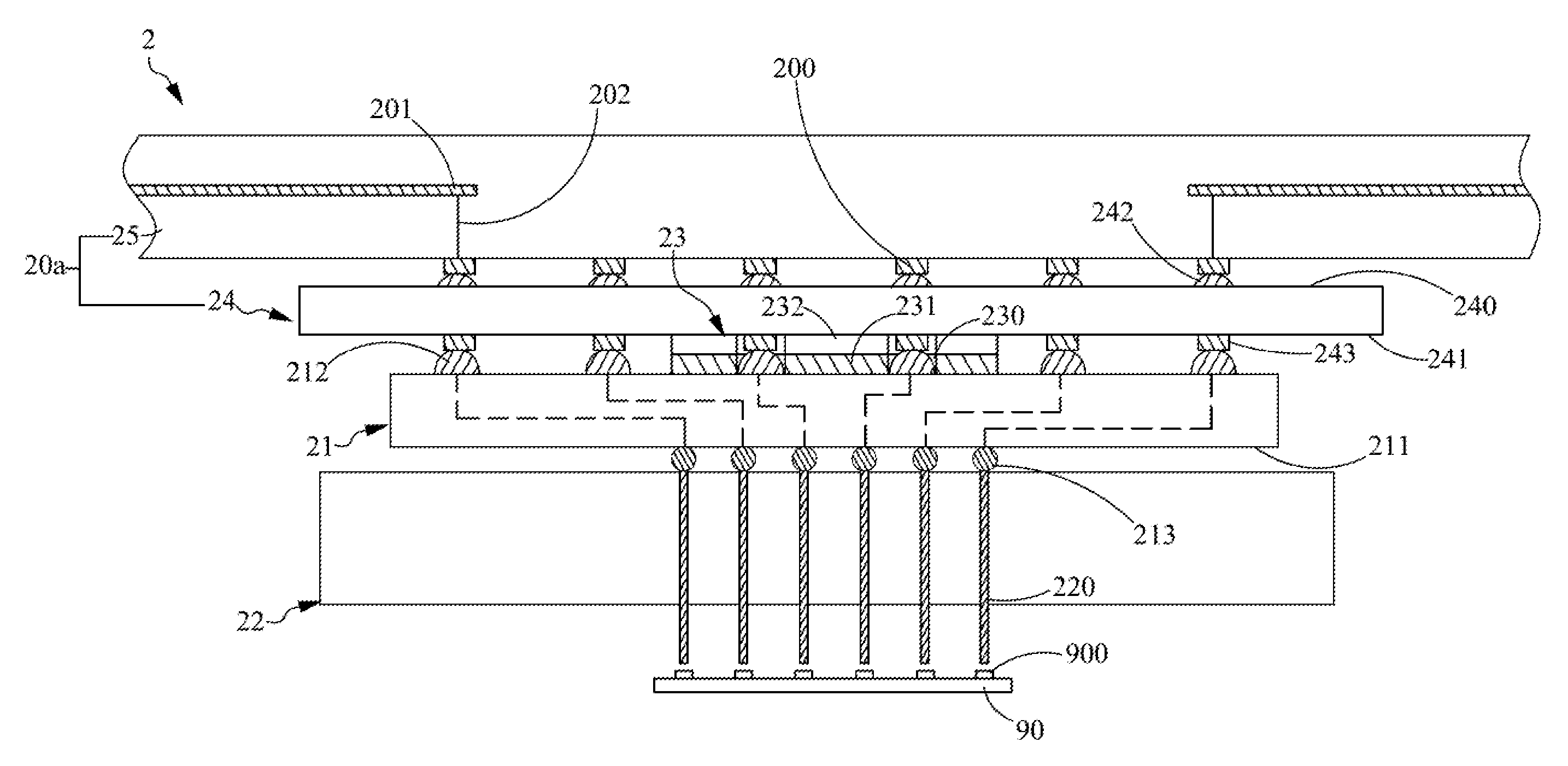
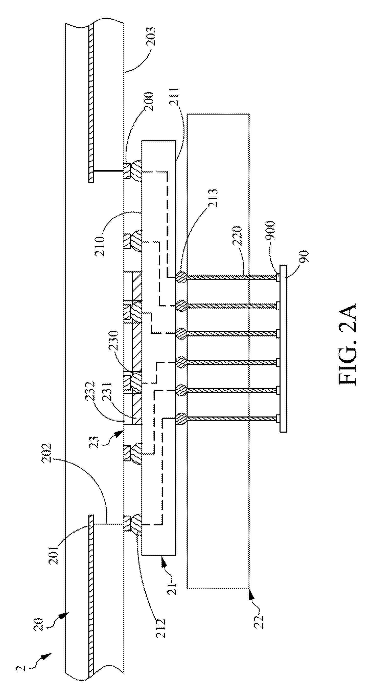
[0034]Please refer to FIG. 2A, which is a schematic diagram showing an apparatus for probing die electricity according to a first embodiment of the invention. In this first embodiment, the apparatus for probing die electricity 2 comprises: a substrate 20, a converting plate 21, a needle module 22 and a reinforcement structure 23. The substrate 20 in this embodiment is substantially a circuit board and has a plurality of third conductive elements 200 disposed on a surface thereof so as to be used as signal transmission interfaces transceiving between the apparatus for probing die electricity 2 and a tester. In addition, the substrate 20 is configured with a plurality of conductive lines 201, and in this embodiment, the conducti...


PUM


Abstract

A method of forming an apparatus for probing die electricity, which determines a reinforcement structure according to features of a converting plate, and combines the converting plate, reinforcement structure and a substrate for forming the apparatus for probing die electricity. In an embodiment, the apparatus for probing die electricity further comprises a substrate, a converting plate, a needle module and a reinforcement structure. The converting plate comprises two opposite surfaces respectively having a plurality of first and second conductive elements. The needle module comprises a plurality of needles respectively and electrically connected to the plurality second conductive elements. The reinforcement structure is disposed between the converting plate and the substrate.

Description

FIELD OF THE INVENTION[0001]The present invention relates to a chip inspection device, and more particularly, to an apparatus with enforcement structure for probing die electricity and method for forming the same.BACKGROUND OF THE INVENTION[0002]Forming a plurality of integrated circuit chips in a semiconductor wafer generally involves a plurality of processing steps. Because of the complex manufacturing process, defects are inevitably found on some chips. Therefore, before the steps of wafer dicing and separation of the integrated circuit chips from the semiconductor wafer, it is necessary to test the integrated circuit chips to determine whether the integrated circuit chips are defective or not.[0003]Generally speaking, to test an integrated circuit (IC) chip, the IC chip is engaged and probed by a probe needle assembly, where electric signals relating to the electric properties of the IC chip is transmitted to a tester for analysis so as to determine whether the integrated circui...

Claims


Application Information

Patent Timeline
Patent Type & Authority Patents(United States)
IPC IPC(8): G01R31/00G01R1/04G01R31/28
CPCG01R31/2889G01R1/0408G01R1/0416
Inventor LEE, CHUNG-TSEWU, CHIEN-CHOUCHAN, YI-MING
Owner MPI CORP
Why Eureka
Try Eureka