
Optical semiconductor modulator device and optical module

a technology of optical semiconductor and modulator device, which is applied in the direction of optical waveguide light guide, optical light guide, instrument, etc., can solve the problems of difficult to raise the polarization extinction ratio, yield decline, and loss of optical properties, and achieve the effect of improving characteristics

Active Publication Date: 2015-10-20
LUMENTUM JAPAN INC
View PDF37 Cites 9 Cited by
  • Summary
  • Abstract
  • Description
  • Claims
  • Application Information

AI Technical Summary

Benefits of technology

[0008]In recent years, there has been demand for cost-saving, size-saving, and electric power consumption-saving and the like. Therefore, integrated devices are preferable in which each optical component of the polarization multiplexing type optical modulator is integrated on the same substrate. By providing the integrated devices in which each optical component is integrated on the same substrate, the number of the components can be reduced, and coupling loss can be reduced. A polarization rotator constituted by a semiconductor for integrating the polarization rotator is disclosed in IEEE Photonics Technology Letters, Vol. 7, No. 8, 1995, p 893 to 895. However, as disclosed in the above-mentioned document, when manufacturing the polarization rotator with a semiconductor, the optical loss increases, and there is a problem that it is difficult to raise the polarization extinction ratio.
[0009]Furthermore, there is also a problem that yield decreases due to manufacturing errors in the polarization rotator. When the polarization rotator serving as an optical component having the low yield is integrated on the same substrate together with other optical components, the yield of the integrated device also decreases, which makes it difficult to reduce the costs. Furthermore, it is possible to improve the yield of the polarization rotator by adjusting an amount of the polarization rotation of the polarization rotator by causing an electrical refractive index change. However, for that reason, there is a need to place one more electric power source, the testing costs rise, and in this case, the reduction in costs is difficult.
[0027]According to the present invention, a polarization multiplexing type optical semiconductor device having improved characteristics and an optical module including the same are provided.

Problems solved by technology

However, as disclosed in the above-mentioned document, when manufacturing the polarization rotator with a semiconductor, the optical loss increases, and there is a problem that it is difficult to raise the polarization extinction ratio.
Furthermore, there is also a problem that yield decreases due to manufacturing errors in the polarization rotator.
When the polarization rotator serving as an optical component having the low yield is integrated on the same substrate together with other optical components, the yield of the integrated device also decreases, which makes it difficult to reduce the costs.
However, for that reason, there is a need to place one more electric power source, the testing costs rise, and in this case, the reduction in costs is difficult.

Method used


Image

  • Optical semiconductor modulator device and optical module
  • Optical semiconductor modulator device and optical module
  • Optical semiconductor modulator device and optical module

Examples


first embodiment

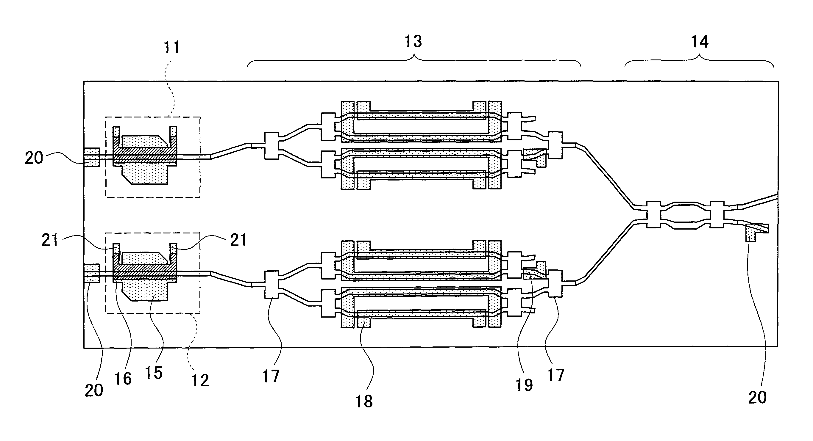
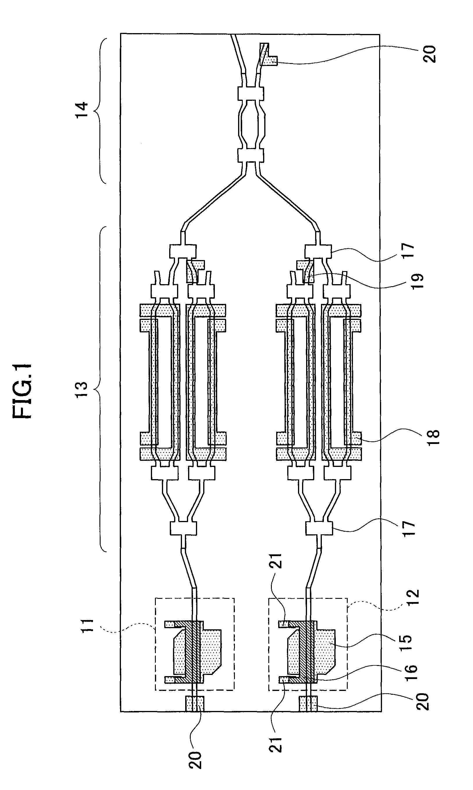
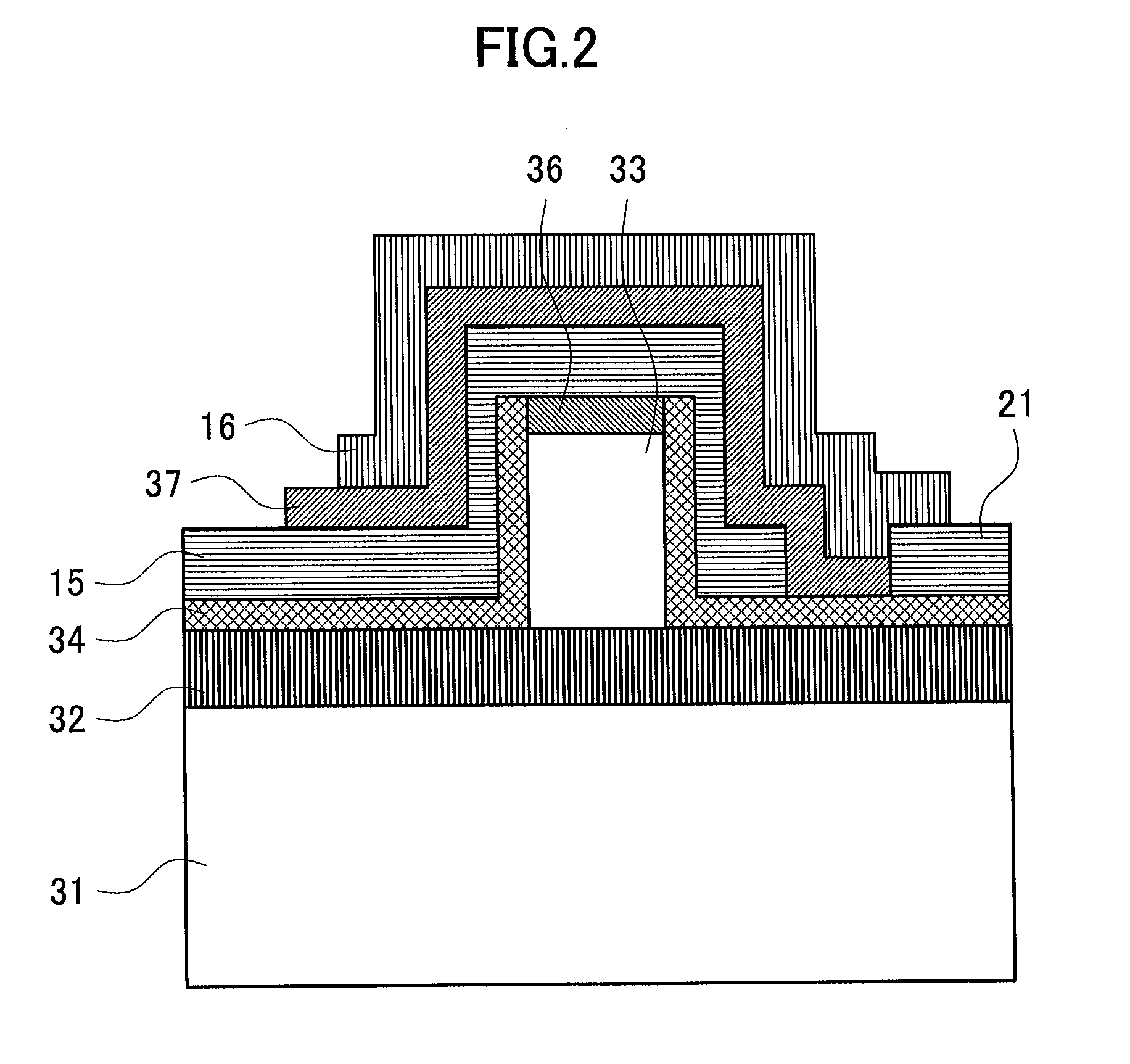
[0046]FIG. 1 is a schematic top view of an optical semiconductor device related to a first embodiment of the present invention. The optical semiconductor device related to the embodiment is a semiconductor optical integrated device in which two LDs, two QPSK modulators (modulation areas 13), a polarization multiplexer 14, and three PDs 20 are included on the same substrate. Herein the two LDs are a first LD11 (a first light source) configured to output light having a TE polarization (a first polarization), and a second LD 12 (a second light source) configured to output light having a TM polarization (a second polarization), and both of them are distributed feedback type (DFB) LDs capable of adjusting the wavelength. In addition, the first LD 11 and the second LD 12 include a LD electrode 15 on a device surface thereof, and include a thin film resistor 16 formed by covering apart of the upper surface of the LD electrode 15. Two electrode pads 21 are provided on both ends of the thin ...

second embodiment

[0074]An optical semiconductor device related to a second embodiment of the present invention differs from the optical semiconductor device related to the first embodiment in that an optical component for detecting whether there is a difference in the wavelengths of the two light sources is further included, but the others are the same configurations as those of the first embodiment. By including such an optical component, there is further an effect that the wavelength of the two light sources can be more precisely controlled in addition to the effect described in the first embodiment.

[0075]FIG. 5 is a schematic top view of the optical semiconductor device related to the present embodiment. On a side of each of the two LDs opposite to the modulation area 13 side, similarly to the PD 20 of the first embodiment, a first PD 40 serving as a light output monitor of the LD is placed so as to be optically connected to the corresponding LD. In addition, an optical waveguide 44 is further ex...

third embodiment

[0087]An optical semiconductor device related to a third embodiment of the present invention is different from the optical semiconductor device related to the second embodiment in that the location in which the ring resonator 42 and the optical waveguide are optically coupled to each other uses not the directional coupler but an MMI multiplexer / demultiplexer. However, the other structures are the same as those of the optical semiconductor device related to the second embodiment.

[0088]FIG. 6 is a schematic top view of the optical semiconductor device related to the present embodiment. As mentioned above, the MMI multiplexer / demultiplexer 45 is placed in the coupling location of the ring resonator 42 and the optical waveguide. The MMI multiplexer / demultiplexer 45 related to the present embodiment has a rectangular shape that is extended in an optical axial direction at a predetermined width by a predetermined length. In addition, the MMI multiplexers / demultiplexers 45 in which the opt...


PUM

PropertyMeasurementUnit
transmission distancesaaaaaaaaaa

Abstract

In an optical semiconductor device related to the present invention, a first light source outputting light having a first polarization, a second light source outputting light having a second polarization, a first optical modulator being optically connected to an output side of the first light source and modulating the light that is output from the first light source to output a light signal, a second optical modulator being optically connected to an output side of the second light source and modulating the light that is output from the second light source to output a light signal, and an optical multiplexer coupling the light signal that is output from the first optical modulator with the light signal that is output from the second optical modulator to output a coupled light signal, are integrated on a semiconductor substrate together.

Description

CROSS-REFERENCE TO RELATED APPLICATION[0001]The present application claims priority from Japanese application JP 2012-029784, filed on Feb. 14, 2012, the content of which is hereby incorporated by reference into this application.BACKGROUND OF THE INVENTION[0002]1. Field of the Invention[0003]The present invention relates to a polarization multiplexing type optical semiconductor modulator device, and an optical module including the same. Particularly, the present invention relates to an improvement in characteristics of a polarization multiplexing type semiconductor optical integrated device.BACKGROUND ART[0004]2. Description of the Related Art[0005]In recent years, optical modulator devices have been used which realize the polarization multiplexing type. In the related art, such optical modulators mainly include a demultiplexer, two modulators, a polarization rotator, and a polarization multiplexer. Input light is divaricated into two beams of light having the same polarization by a...

Claims


Application Information

Patent Timeline
Patent Type & Authority Patents(United States)
IPC IPC(8): G02F1/225G02B6/293G02F1/01G02B6/12G02F1/21
CPCG02F1/2257G02B6/12007G02F1/011G02F1/225G02B6/29352G02B2006/12159G02F2001/212G02F1/212
Inventor HAYASHI, HIROAKIARIMOTO, HIDEO
Owner LUMENTUM JAPAN INC
Learn More