Array substrate for liquid crystal display device and three-dimensional image display device including the same
a liquid crystal display and array substrate technology, applied in semiconductor devices, optics, instruments, etc., can solve the problems of unsatisfactory color image display, deterioration of display quality of ips mode lcd devices, and deterioration of display quality of two-dimensional image and three-dimensional image brightness, so as to improve the brightness of two-dimensional image
- Summary
- Abstract
- Description
- Claims
- Application Information
AI Technical Summary
Benefits of technology
Problems solved by technology
Method used
Image


Examples
first embodiment
[0043]FIG. 5 is a plan view showing an array substrate for an in-plane switching (IPS) mode liquid crystal display (LCD) device according to a
[0044]In FIG. 5, first and second gate lines GL1 and GL2 and a common line CL are formed on a substrate 201. The first and second gate lines GL1 and GL2 and the common line CL are spaced apart from and parallel to each other, and the second gate line GL2 is disposed between the first gate line GL1 and the common line CL. In addition, first and second data lines DL1 and DL 2 crossing the first and second gate lines GL1 and GL2 and the common line CL are formed on the substrate 201.
[0045]In the substrate 201, a pixel region P is defined as an area surrounded by the first and second data lines DL1 and DL2 and first and second virtual lines VL1 and VL2 corresponding to end portions of first pixel electrodes 260 and end portions of second pixel electrodes 268, respectively. As a result, the pixel region P includes a first area A1 surrounded by the ...
second embodiment
[0056]For the purpose of further improving brightness, an array substrate for an IPS mode LCD device is suggested in a
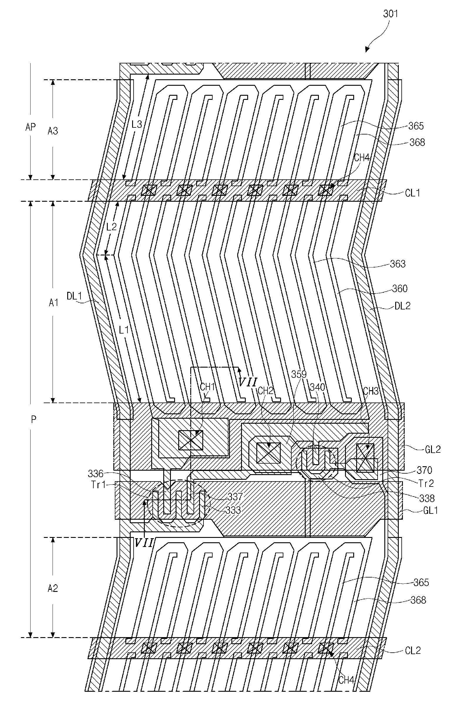
[0057]FIG. 6 is a plan view showing an array substrate for an in-plane switching (IPS) mode liquid crystal display (LCD) device according to a second embodiment.
[0058]In FIG. 6, first and second gate lines GL1 and GL2 and first and second common lines CL1 and CL2 are formed on a substrate 301. The first and second gate lines GL1 and GL2 and the first and second common lines CL1 and CL2 are spaced apart from and are parallel to each other. The second gate line GL2 is disposed between the first gate line GL1 and the first common line CL1, and the first gate line GL1 is disposed between the second gate line GL2 and the second common line CL2. In addition, first and second data lines DL1 and DL2 crossing the first and second gate lines GL1 and GL2 and the first and second common lines CL1 and CL2 are formed on the substrate 301.
[0059]In the substrate 301, a pixel region ...
PUM
| Property | Measurement | Unit |
|---|---|---|
| viewing angle | aaaaa | aaaaa |
| area | aaaaa | aaaaa |
| phase difference | aaaaa | aaaaa |
Abstract
Description
Claims
Application Information