Power semiconductor module and method of manufacturing the same
a technology of power semiconductor and manufacturing method, which is applied in the direction of semiconductor devices, semiconductor/solid-state device details, electrical apparatus, etc., can solve the problems of disconnection of wires or shirt circuits, and achieve the effect of preventing wire disconnection or short circui
- Summary
- Abstract
- Description
- Claims
- Application Information
AI Technical Summary
Benefits of technology
Problems solved by technology
Method used
Image
Examples
first embodiment
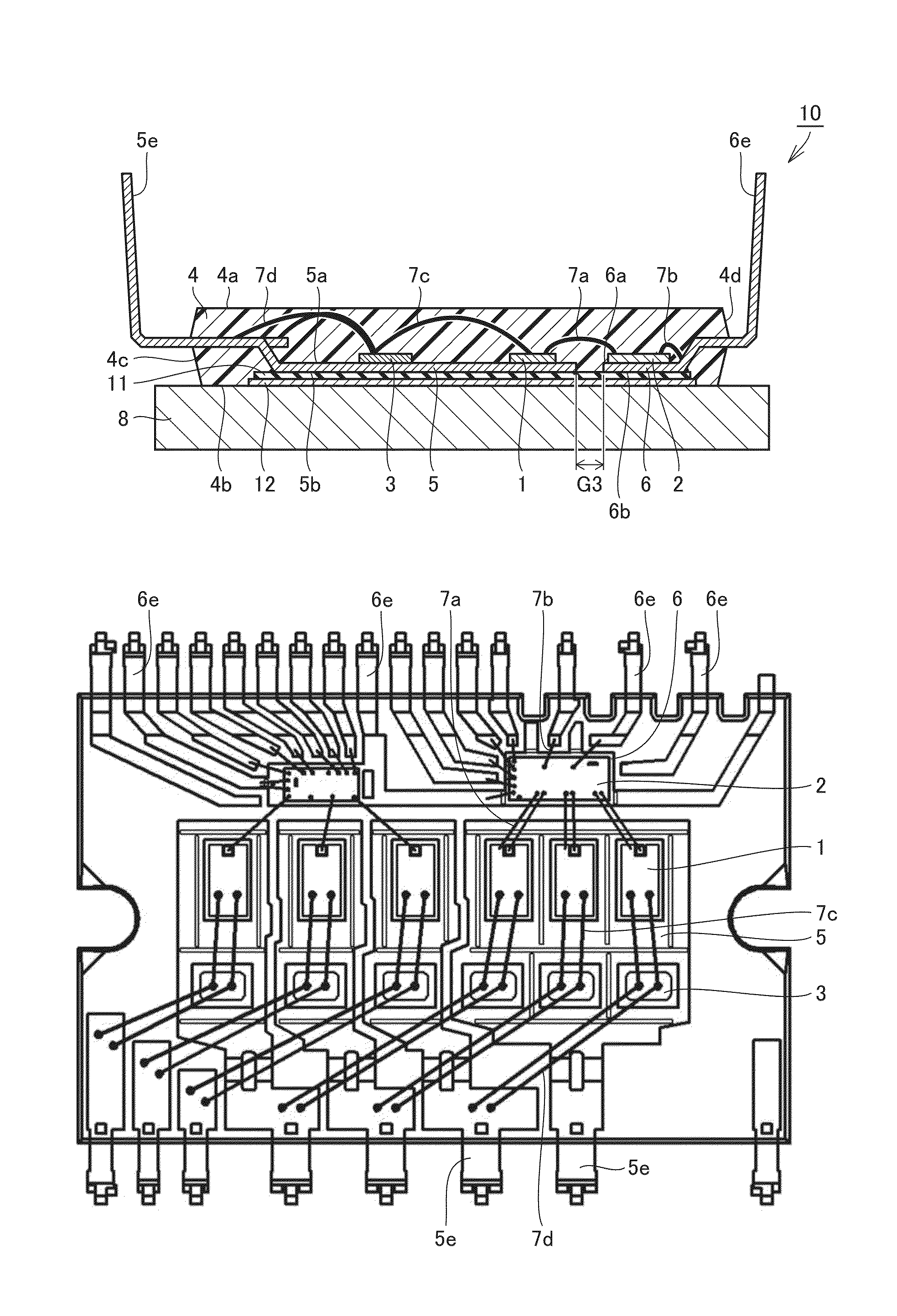
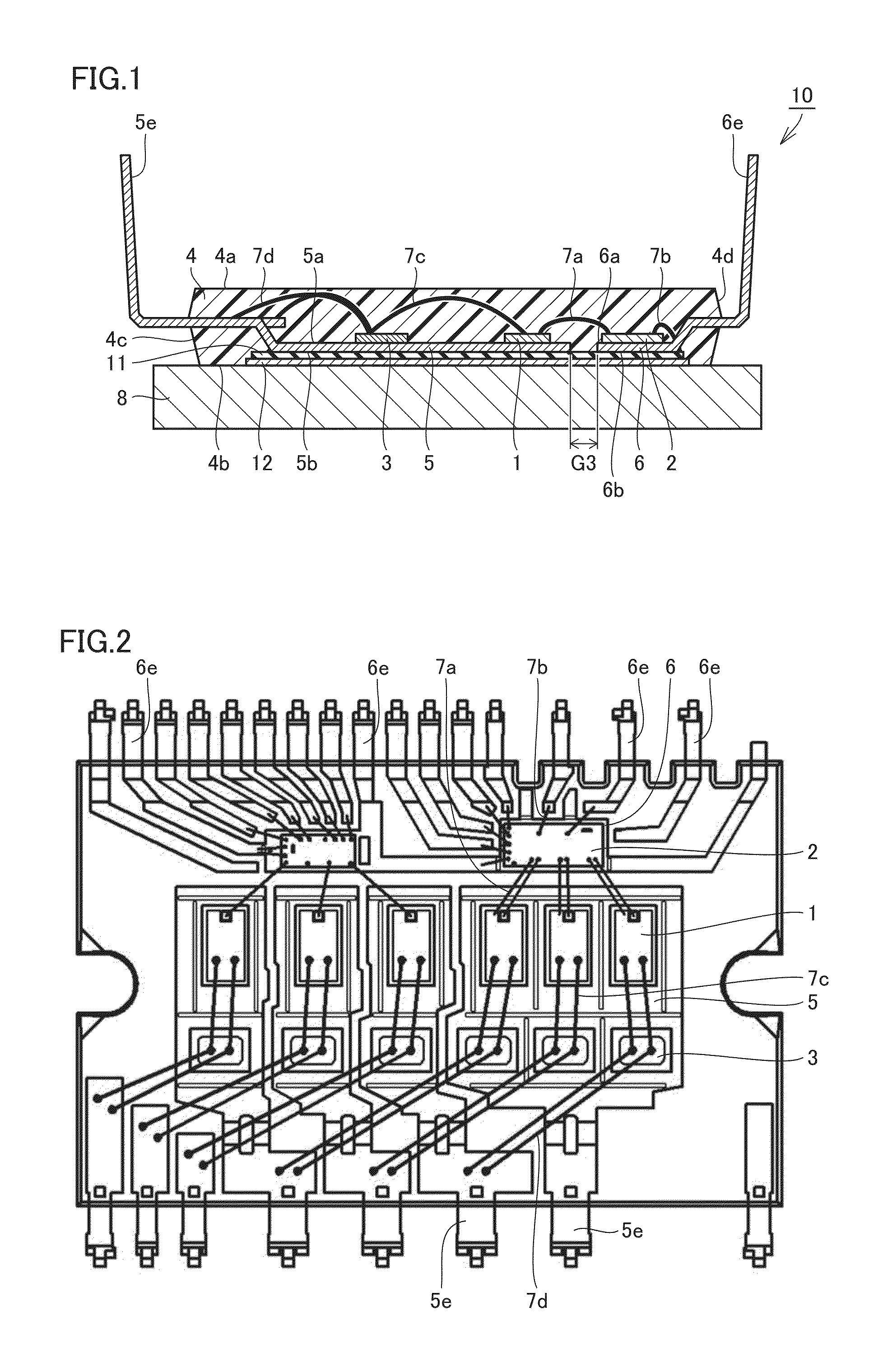
[0026]Referring to FIGS. 1 and 2, a configuration of a power semiconductor module according to a first embodiment will be described. A power semiconductor module 10 according to the first embodiment mainly includes an IGBT 1, an IC (Integrated Circuit) 2, an FWDi (Free Wheeling Diode) 3, a first frame portion 5, a second frame portion 6, a wire 7a, and an insulator portion 4.
[0027]The first frame portion 5 has a first surface 5a and a second surface 5b opposed to each other. Power semiconductor elements such as IGBT 1 and FWDi 3 are mounted on first surface 5a of first frame portion 5. IGBT 1 and FWDi 3 are each joined to first surface 5a, for example, with a joint member such as solder.
[0028]The second frame portion 6 has a third surface 6a and a fourth surface 6b opposed to each other. IC 2 that is a control integrated circuit for controlling the power semiconductor elements is mounted on third surface 6a of second frame 6. The back surface of IC 2 is joined to third surface 6a, f...
second embodiment
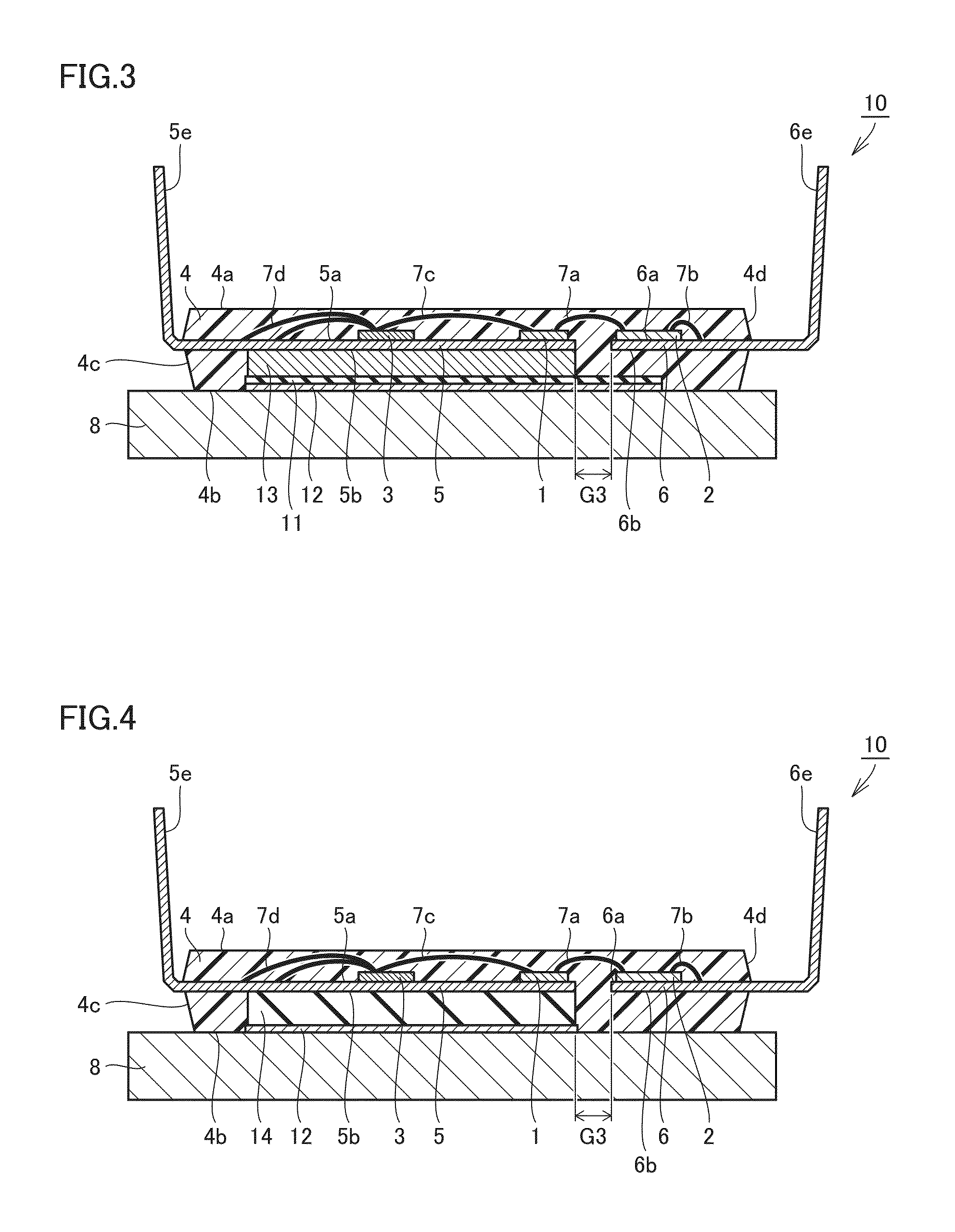
[0046]Referring to FIGS. 3 and 5, a configuration of a power semiconductor module according to a second embodiment will now be described. The configuration of power semiconductor module 10 according to the second embodiment differs from the configuration of the power semiconductor module according to the first embodiment in that a block portion 13 made of copper is arranged between first frame portion 5 and insulating sheet 11. The other configuration is the same as the first embodiment.
[0047]In power semiconductor module 10 according to the second embodiment, block portion 13 made of copper is arranged in contact with second surface 5b of first frame portion 5 and insulating sheet 11. First frame portion 5 having IGBT 1 and FWDi 3 mounted thereon and second frame portion 6 having IC 2 mounted thereon are located at the same height in the direction normal to first surface 5a of the first frame portion. Second frame portion 6 is in contact with insulating sheet 11 with insulator port...
third embodiment
[0050]Referring to FIGS. 4 and 5, a configuration of a power semiconductor module according to a third embodiment will be described. The configuration of the power semiconductor module according to the third embodiment differs from the configuration of the power semiconductor module according to the second embodiment in that block portion 13 has a DBC (Direct Bonded Copper) structure because of inclusion of ceramic. The other configuration is the same as the second embodiment.
[0051]The DBC has a ceramic base arranged between two copper plates and bonded to the copper plates. Specifically, power semiconductor module 10 according to the third embodiment has a block portion arranged between first frame portion 5 made of copper and metal plate 12 made of copper. The block portion is formed of a ceramic base 14 of aluminum oxide (Al2O3), aluminum nitride (AlN), or the like. First frame portion 5 having IGBT 1 and FWDi 3 mounted thereon and second frame portion 6 having IC 2 mounted there...
PUM
 Abstract
Description
Claims
Application Information


