Semiconductor device and data processing system

a technology of semiconductor devices and data processing systems, applied in computing, instruments, climate sustainability, etc., can solve the problems of frequent reading of instructions from nor flash memory, and achieve the effects of expanding memory capacity, high speed, and low cos

Active Publication Date: 2015-11-03
HITACHI LTD
View PDF20 Cites 0 Cited by
  • Summary
  • Abstract
  • Description
  • Claims
  • Application Information

AI Technical Summary

Benefits of technology

[0014]According to the present invention, a data processing system capable of ensuring expandability of memory capacity at a high speed and low cost keeping a data read latency constant, and having excellent usability can be achieved.BRIEF DESCRIPTIONS OF THE DRAWINGS
[0015]FIG. 1 is a diagram showing one example of structure of a data processing system to which the present invention is applied;
[0016]FIG. 2 is a diagram showing one example of structure of a data processing device configuring the data processing system to which the present invention is applied;
[0017]FIG. 3 is a diagram showing one example of a configuration of a memory;
[0018]FIG. 4 is a diagram showing one example of a circuit block of a memory circuit mounted in the memory;
[0019]FIG. 5 is a diagram showing one example of structure of the memory;

Problems solved by technology

That is, it has been found out that random reading of instructions from the NOR flash memory frequently occurs.

Method used


Image

  • Semiconductor device and data processing system
  • Semiconductor device and data processing system
  • Semiconductor device and data processing system

Examples


first embodiment

[0064](First Embodiment)

[0065]A data processing system which is a first embodiment to which the present invention is applied will be described with reference to FIGS. 1 to 30.

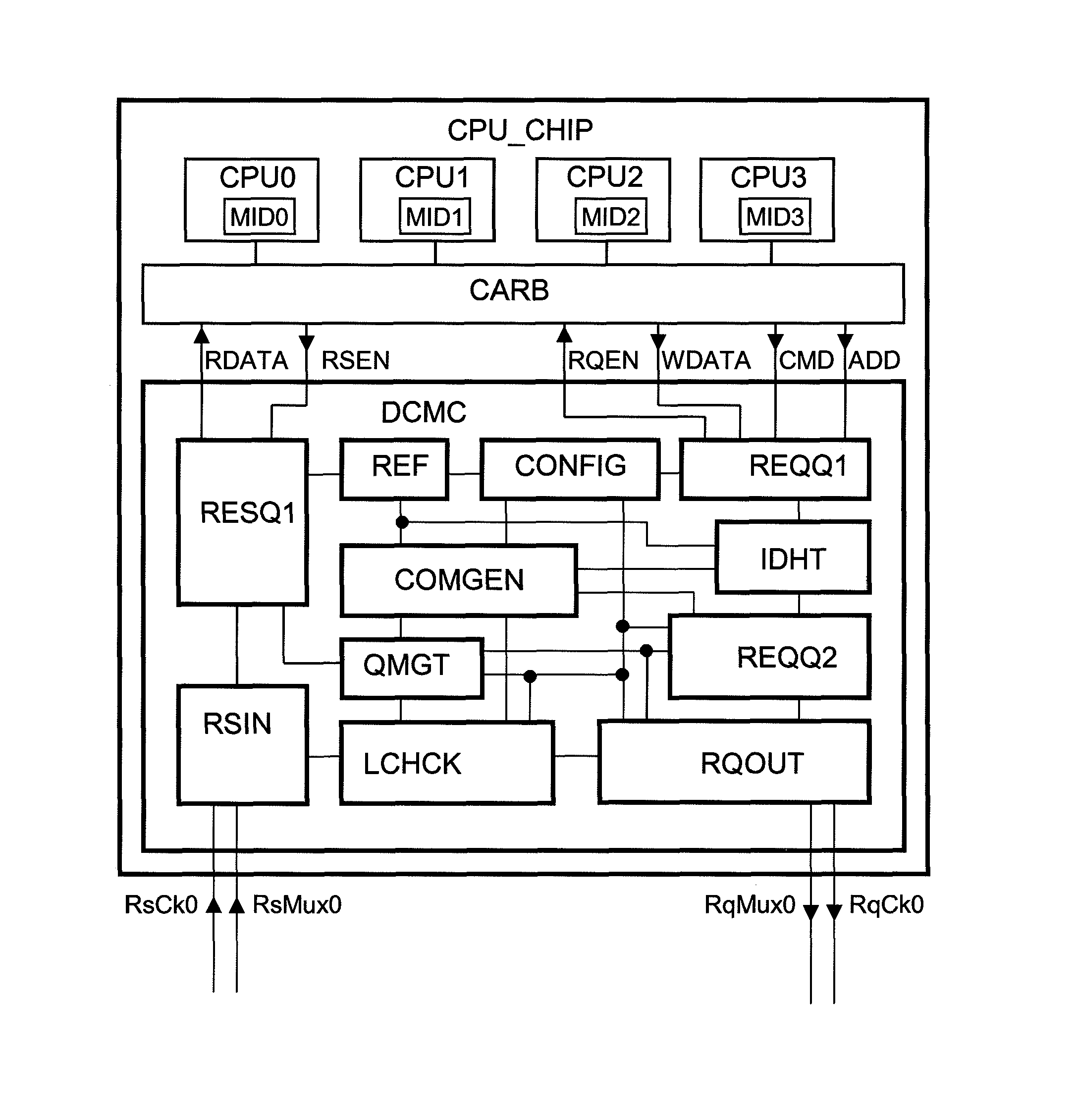
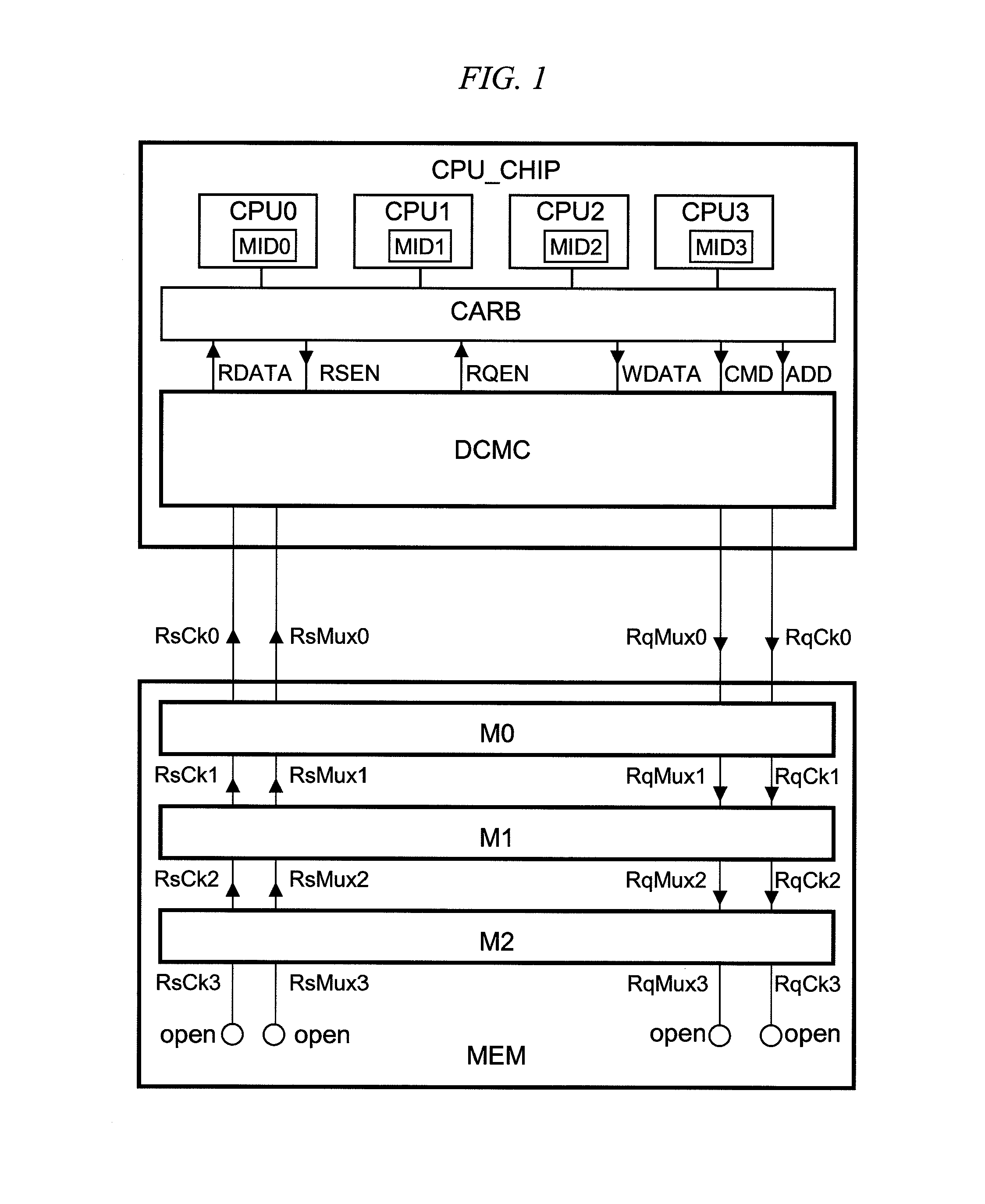
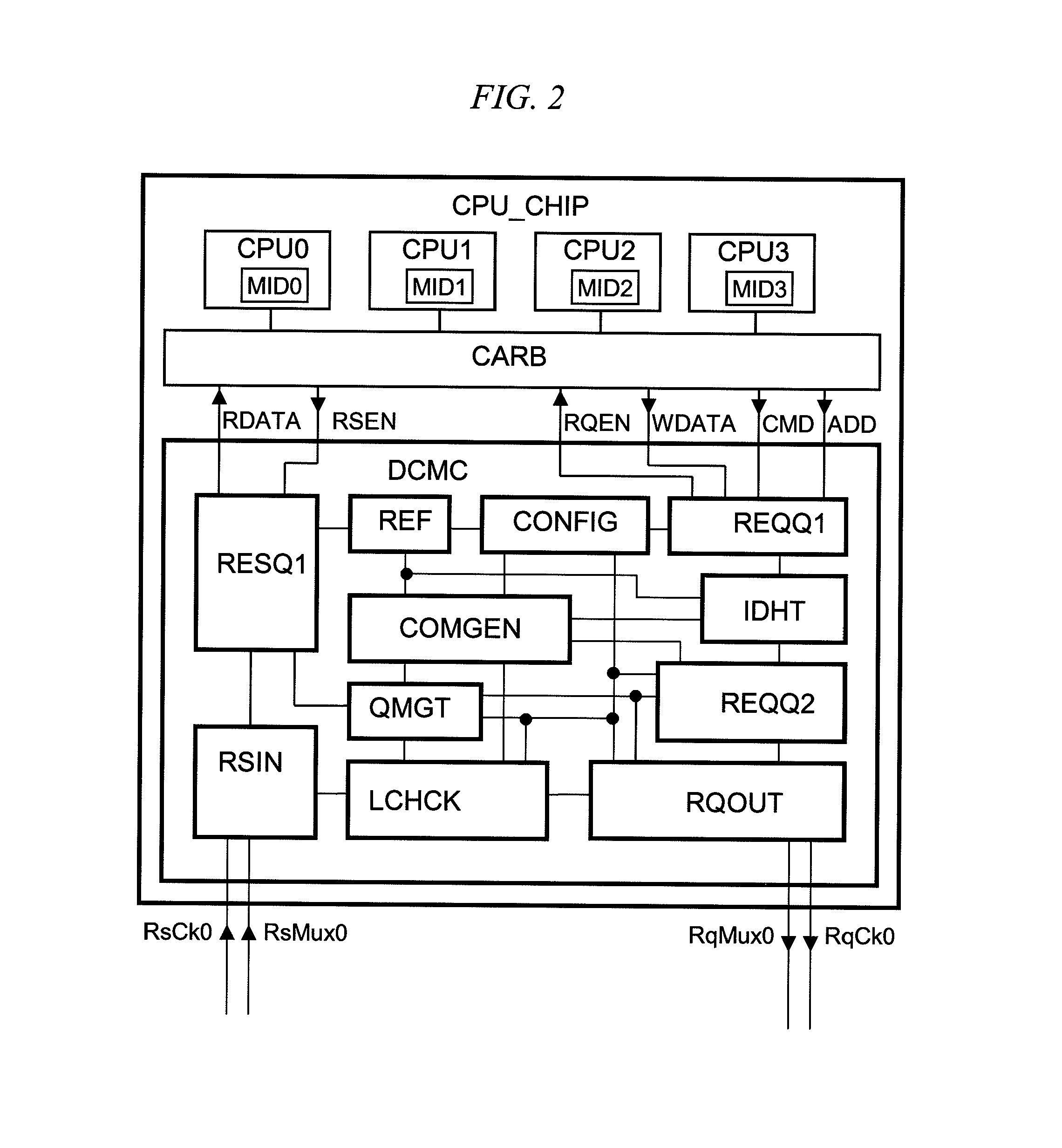
[0066]FIG. 1 is a block diagram showing one example of a configuration of a data processing system formed of a data processing device CPU_CHIP and a memory module MEM according to the first embodiment to which the present invention is applied. Also, FIG. 2 is a block diagram showing one example of a configuration of the data processing device CPU_CHIP. Each component will be described below.

[0067]The data processing device CPU_CHIP includes data processing circuits CPU0, CPU1, CPU2, and CPU3, an arbitration circuit CARB, and a memory control circuit DCMC. The memory module MEM includes memory devices (memories) M0, M1, and M2. In addition, the data processing device CPU_CHIP and the memories M0, M1, and M2 are connected in series. The data processing circuit CPU0 mounts a master number register MID0, the data p...

second embodiment

[0443](Second Embodiment)

[0444]A data processing system of a second embodiment to which the present invention is applied will be described with reference to FIGS. 31 to 35. FIG. 31 is a block diagram showing an example of a structure of a data processing system composed of a data processing device CPU_CHIP1 and a memory module MEM1 in the second embodiment to which the present invention is applied. Also, FIG. 32 is a block diagram showing an example of a structure of the data processing device CPU_CHIP1. The memory module MEM1 includes memories M10, M11, and M12. Also, the data processing device CPU_CHIP1 and the memories M10, M11, and M12 are connected in series. Furthermore, FIG. 33 is a block diagram showing an example of a structure of the memory M10, FIG. 34 is a block diagram showing an example of a structure of the memory M11, and FIG. 35 is a block diagram showing an example of a structure of the memory M12.

[0445]Also, as a clock mode for operating the data processing device...

third embodiment

[0460](Third Embodiment)

[0461]FIG. 36 shows a third embodiment of the present invention. This embodiment describes a data processing system including a data processing device CPU_CHIP and a memory module MEM3. In the present embodiment, an example of the data processing system of a source synchronous clock mode is shown. The data processing device CPU_CHIP is similar to that shown in FIGS. 1 and 2. The memory module MEM3 includes a memory M31, a memory M32, and a memory M33. RqCk0, RqCk1, and RqCk2 are request clocks, and RsCk0, RsCk1, and RsCk2 are response clocks. RqMux0, RqMux1, and RqMux2 are request signals, and RsMux0, RsMux1, and RsMux2 are response signals. PNS and CNS are connection check signals between the data processing device CPU_CHIP and the memory M33.

[0462]The memory M31 is composed of an interface circuit chip RQRSIF31 and a plurality of volatile memory chips VLM31. The interface circuit chip RQRSIF31 is equipped with functions equivalent to all circuits in the mem...


PUM


Abstract

A high-speed, low-cost data processing system capable of ensuring expandability of memory capacity and having excellent usability while keeping constant latency is provided. The data processing system is configured to include a data processing device, a volatile memory, and a non-volatile memory. As the data processing device, the volatile memory, and the non-volatile memory are connected in series and the number of connection signals are reduced, the speed is increased while keeping expandability of memory capacity. The data processing device measures latency and performs a latency correcting operation to keep the latency constant. When data in the non-volatile memory is transferred to the volatile memory, error correction is performed to improve reliability. The data processing system formed of these plurality of chips is configured as a data processing system module in which the chips are disposed so as to be multilayered each other and are connected by a ball grid array (BGA) or a technology of wiring these chips.

Description

TECHNICAL FIELD[0001]The present invention relates to technologies for semiconductor devices and, in particular, to technology effectively applied to a data processing system including a non-volatile memory and a data processing device, and a method of controlling a memory module.BACKGROUND ARTProblems to be Solved by the Invention[0002]In recent years, as shown in Patent Document 1, in order to decrease the number of signals between a data processing device and memories, to improve an operating frequency, and to increase a data transfer speed, a data processing system is suggested, in which a data processing device and a plurality of memories are connected in series. Specifically, each memory has request queues retaining requests transmitted from the data processing device and response queues retaining responses to the data processing device. The response queues include a response queue retaining a response from its own memory and a response queue retaining a response from a memory...

Claims


Application Information

Patent Timeline
Patent Type & Authority Patents(United States)
IPC IPC(8): G06F12/00G06F13/16
CPCG06F13/1689Y02B60/1228Y02D10/00
Inventor MIURA, SEIJI
Owner HITACHI LTD
Why Eureka
Try Eureka