Eureka AIR delivers breakthrough ideas for toughest innovation challenges, trusted by R&D personnel around the world.

Mask assembly for thin film vapor deposition and manufacturing method thereof

a technology of vapor deposition and mask, which is applied in the direction of vacuum evaporation coating, electroluminescent light sources, coatings, etc., can solve the problems of deposition defect, increased wrinkles, and wrinkles in the mask, and achieve the effect of effectively removing the wrinkles of the unit mask and improving the deposition quality of the thin film

Active Publication Date: 2015-11-17
SAMSUNG DISPLAY CO LTD
View PDF11 Cites 6 Cited by
  • Summary
  • Abstract
  • Description
  • Claims
  • Application Information

AI Technical Summary

Benefits of technology

[0010]An aspect of the present invention provides a mask assembly that increases deposition quality of a thin film by suppressing a winkle generated in a unit mask and a manufacturing method thereof for the mask assembly of a division mask method.
[0022]The unit mask having the wrinkle generated by the tension of the first direction is expanded in the second direction thereby effectively removing the wrinkle of the unit mask. Accordingly, the deformation of the pattern opening of the unit mask by the wrinkle may be suppressed, thereby improving the deposition quality of the thin film.

Problems solved by technology

The unit mask is applied with a tension force in one direction such that the unit mask is elongated in the length direction of the tension direction, however, a contraction is generated in a direction crossing the tension direction, that is, a width direction, and thereby the entire mask may be wrinkled.
This wrinkle becomes more serious as a width of the unit mask is increased.
The wrinkle that is generated at the ends of the unit mask is expanded to the center of the unit mask in which an opening is positioned thereby generating a deposition defect.

Method used


Image

  • Mask assembly for thin film vapor deposition and manufacturing method thereof
  • Mask assembly for thin film vapor deposition and manufacturing method thereof
  • Mask assembly for thin film vapor deposition and manufacturing method thereof

Examples


Embodiment Construction

[0032]The present invention will be described more fully hereinafter with reference to the accompanying drawings, in which exemplary embodiments of the invention are shown. As those skilled in the art would realize, the described embodiments may be modified in various different ways, all without departing from the spirit or scope of the present invention.

[0033]Unless explicitly described to the contrary, the word “comprise” and variations such as “comprises” and “comprising” will be understood to imply the inclusion of stated elements but not the exclusion of any other elements. In addition, it will be understood that when an element such as a layer, film, region, or substrate is referred to as being “on” another element, it can be directly on the other element or intervening elements may also be present. Throughout this specification, it is understood that the term “on” and similar terms are used generally and are not necessarily related to a gravitational reference.
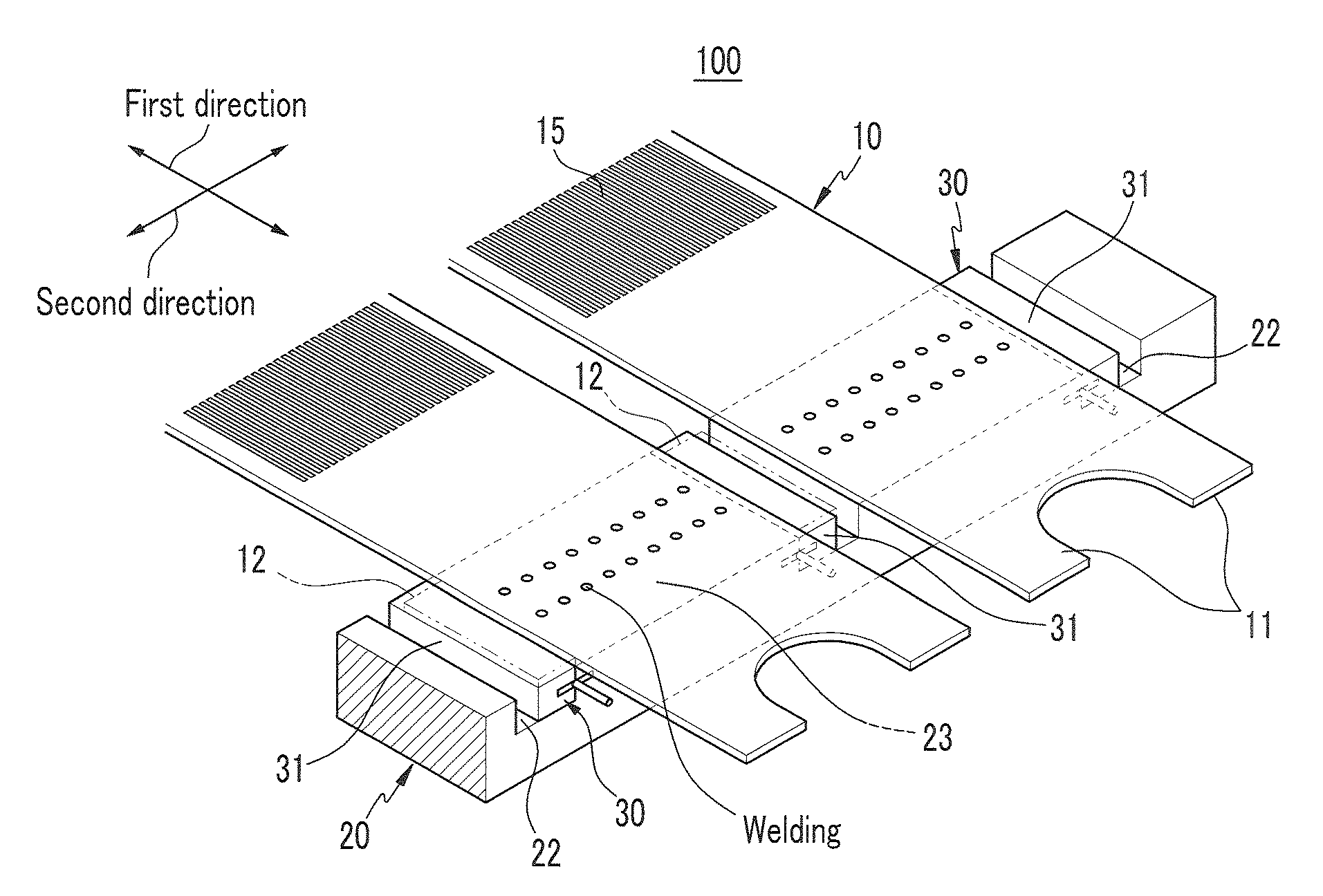
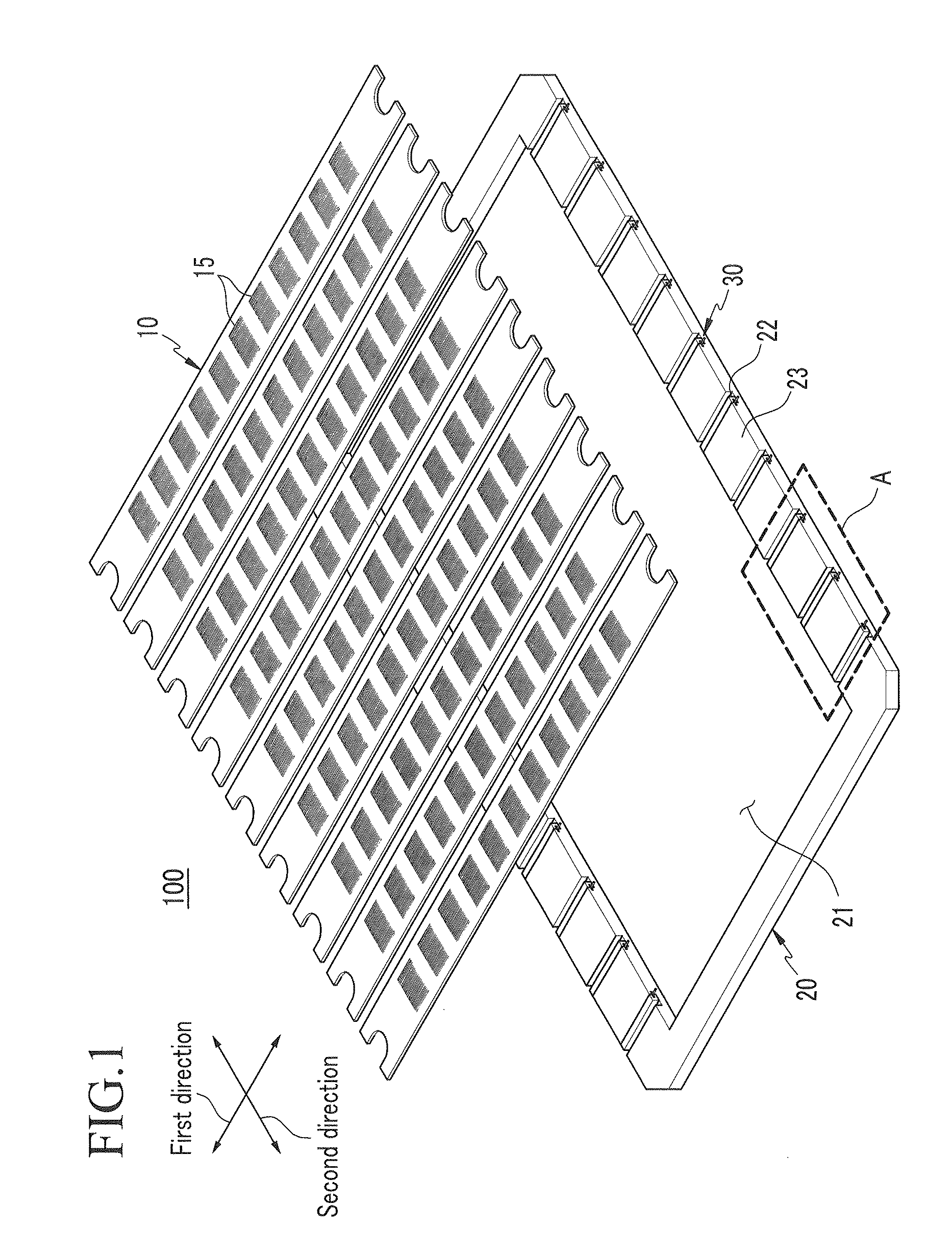
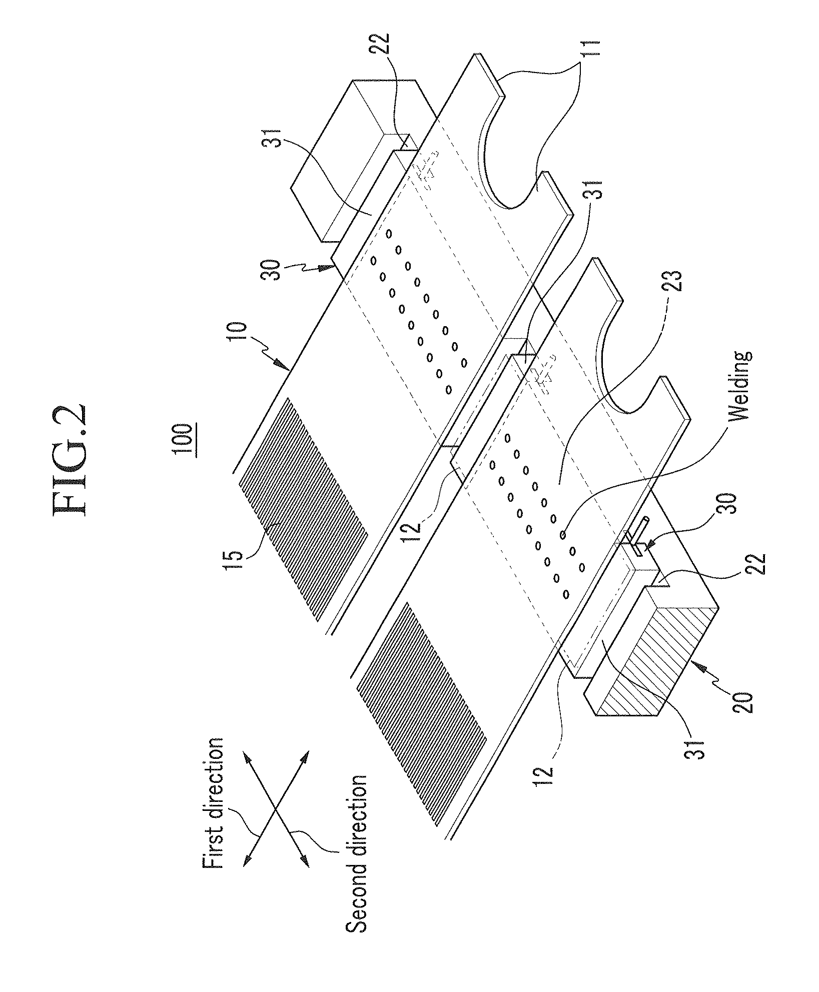
[0034]FIG. 1 is...


PUM

PropertyMeasurementUnit
tension forceaaaaaaaaaa
tensionaaaaaaaaaa
widthaaaaaaaaaa

Abstract

A mask assembly for a thin film deposition includes: a frame main body forming an opening; a plurality of unit masks having both ends fixed to the frame main body in a state that a tension force is applied in a first direction; and an end tension unit installed to the frame main body. The end tension unit moves according to a second direction crossing the first direction between two neighboring unit masks among a plurality of unit masks for tensioning of the unit mask in the second direction.

Description

CLAIM OF PRIORITY[0001]This application makes reference to, incorporates the same herein, and claims all benefits accruing under 35 U.S.C. §119 from an application earlier filed in the Korean Intellectual Property Office on 15 Nov. 2012 and there duly assigned Serial No. 10-2012-0129596.BACKGROUND OF THE INVENTION[0002]1. Field of the Invention[0003]An embodiment of the present invention relates generally to a mask assembly, and more particularly, to a mask assembly used in a thin film deposition process such as an organic emission layer or a metal layer, and a manufacturing method thereof.[0004]2. Description of the Related Art[0005]As a flat panel display device, a liquid crystal display (LCD) device and an organic light emitting diode (OLED) display device are widely used. The flat panel display device includes a metal layer of a predetermined pattern, and in a case of the organic light emitting diode (OLED) display device, an organic emission layer of the predetermined pattern i...

Claims


Application Information

Patent Timeline
Patent Type & Authority Patents(United States)
IPC IPC(8): B05C11/00C23C14/04H01L51/00
CPCC23C14/042H01L51/0011Y10T29/49826H10K71/166H05B33/10H10K71/00
Inventor KIM, YONG-HWAN
Owner SAMSUNG DISPLAY CO LTD
Why Eureka
Eureka Blog
Learn More