Eureka AIR delivers breakthrough ideas for toughest innovation challenges, trusted by R&D personnel around the world.

Vacuum processing apparatus

Inactive Publication Date: 2011-12-22
MITSUBISHI HEAVY IND LTD
View PDF9 Cites 7 Cited by
  • Summary
  • Abstract
  • Description
  • Claims
  • Application Information

AI Technical Summary

Benefits of technology

[0044]With the vacuum processing apparatus according to the present invention, because a substrate, a gas supplying portion and a discharge chamber are sequentially disposed inside a low-pressure vessel, and because an exhaust portion communicates with the low-pressure vessel at a position thereof such that this position and the gas supplying portion are disposed of either side of the discharge chamber, an advantage is afforded in that the quality of a deposited film is increased, the area thereof is increased, and deposition speed is increased.

Problems solved by technology

On the other hand, the performance of solar cells having amorphous silicon films (hereinafter, referred to as “a-Si solar cells”) has been known to deteriorate due to photodegradation.
Due to this problem, there has been a problem in that it is difficult to increase the deposition speed of the amorphous silicon films for a-Si solar cells.
However, in the deposition of amorphous silicon films by employing the VHF band frequency, although the photodegradation is inhibited, it is not adequate, and the performance of a-Si solar cells deteriorates beyond a tolerable level.

Method used


Image

  • Vacuum processing apparatus
  • Vacuum processing apparatus
  • Vacuum processing apparatus

Examples


first embodiment

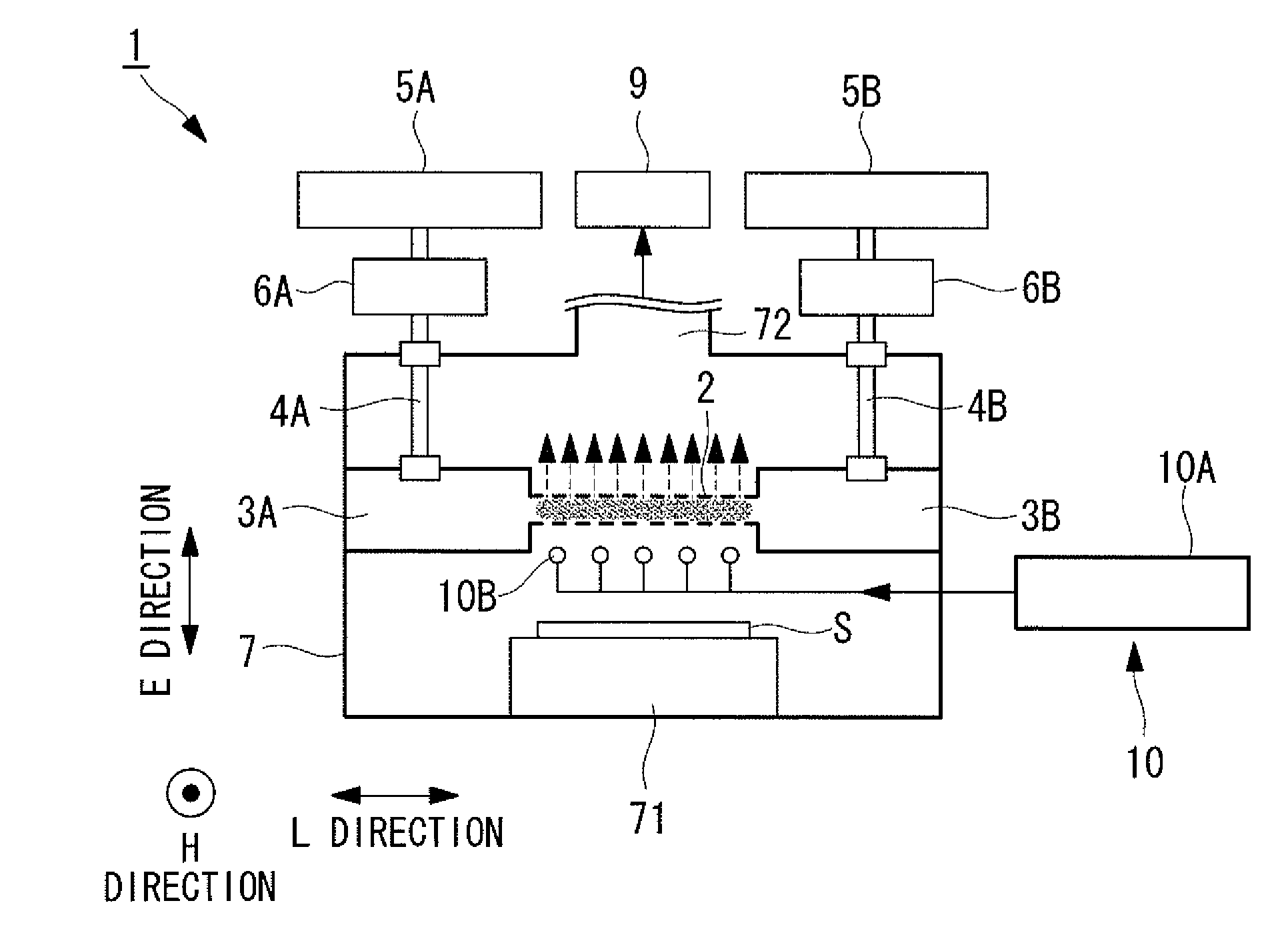
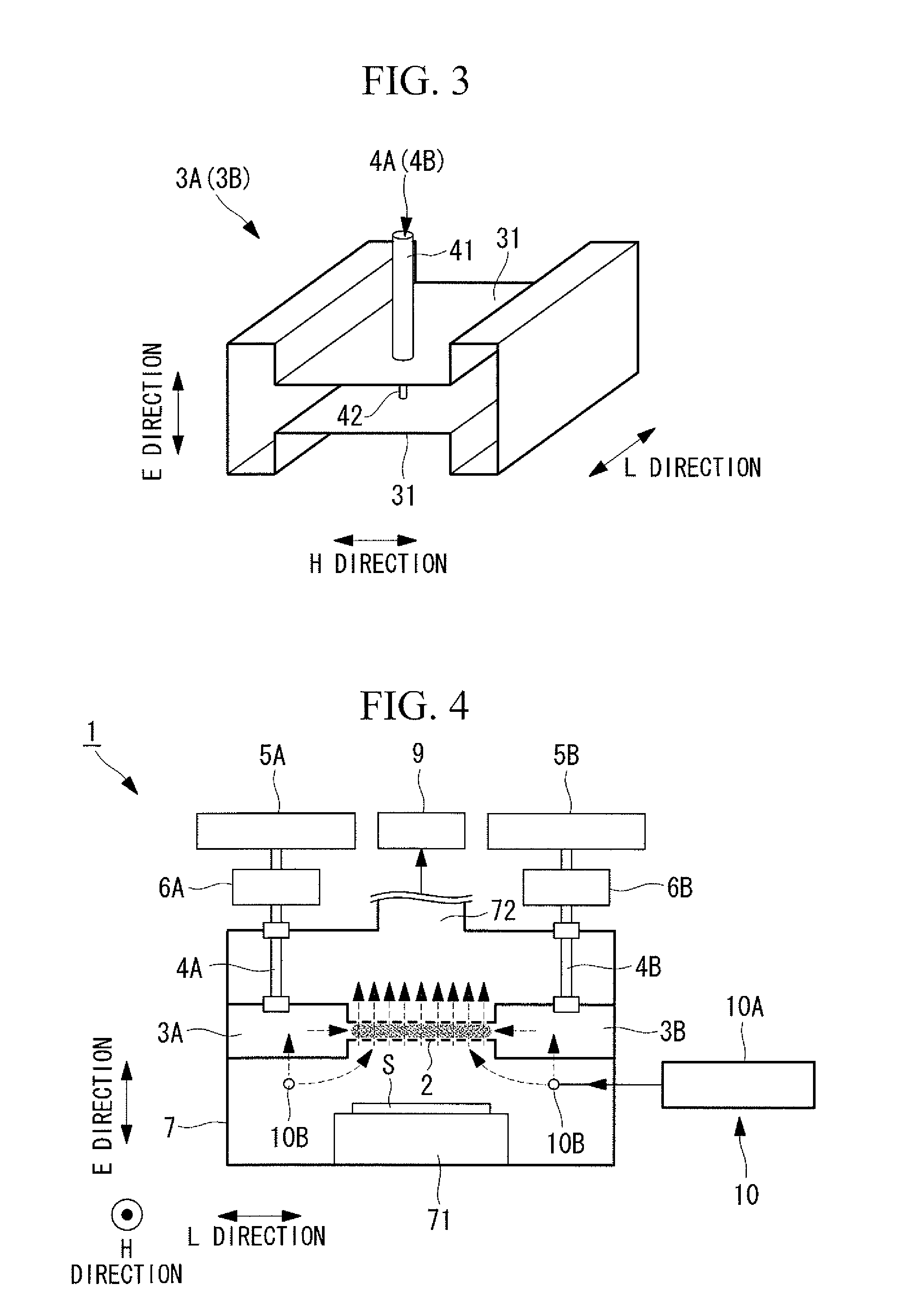
[0053]A deposition apparatus according to a first embodiment of the present invention will be described below with reference to FIGS. 1 to 3.

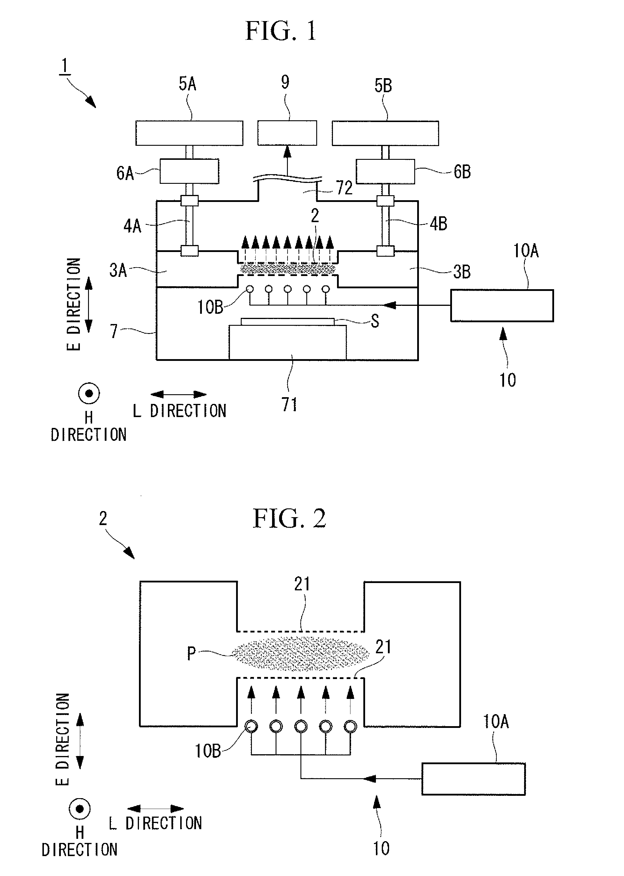
[0054]FIG. 1 is a schematic diagram for explaining, in outline, the configuration of the deposition apparatus according to this embodiment. FIG. 2 is a partial sectional view for explaining a processing chamber in FIG. 1.

[0055]In this embodiment, a case will be described in which the present invention is applied to a deposition apparatus (vacuum processing apparatus) 1 that is capable of performing deposition processing of films formed of amorphous silicon, crystalline silicon such as microcrystalline silicon, silicon nitride and the like which are employed in amorphous solar cells, microcrystalline solar cells, TFTs (Thin Film Transistors) for liquid crystal displays and the like for a large-area substrate whose area is 1 m2 or greater.

[0056]As shown in FIG. 1, the deposition apparatus 1 is mainly provided with a processing chamber (discharge ...

second embodiment

[0130]Next, a second embodiment of the present invention will be described with reference to FIG. 6.

[0131]Although the basic configuration of a deposition apparatus of this embodiment is similar to that of the first embodiment, configurations of the processing chamber, the first converter, and the second converter differ from those of the first embodiment. Therefore, in this embodiment, only the vicinity of the processing chamber and the like will be described using FIG. 6, and the descriptions of other components and the like will be omitted.

[0132]FIG. 6 is a diagram for explaining, in outline, the configuration of a deposition apparatus according to a second embodiment of the present invention.

[0133]Components that are same as those in the first embodiment are given the same reference signs, and descriptions thereof will be omitted.

[0134]As shown in FIG. 6, a deposition apparatus (vacuum processing apparatus) 101 is mainly provided with the processing chamber2, a first converter (...

third embodiment

[0148]Next, a third embodiment of the present invention will be described with reference to FIG. 7.

[0149]Although the basic configuration of a deposition apparatus of this embodiment is similar to that of the second embodiment, the configuration of the vacuum vessel differs from that of the second embodiment. Therefore, in this embodiment, only the configuration of the vacuum vessel will be described using FIG. 7, and the descriptions of other components, etc. will be omitted.

[0150]FIG. 7 is a diagram for explaining, in outline, the configuration of a deposition apparatus according to this embodiment.

[0151]Components that are same as those in the second embodiment are given the same reference signs, and descriptions thereof will be omitted.

[0152]As shown in FIG. 7, a deposition apparatus (vacuum processing apparatus) 201 is mainly provided with the processing chamber 2, the first converter 103A, the second converter 103B, the first coaxial line 4A, the first power source 5A, the fir...


PUM

PropertyMeasurementUnit
Pressureaaaaaaaaaa
Flow rateaaaaaaaaaa

Abstract

A discharge chamber formed of a ridge waveguide having ridge electrodes that are disposed facing each other and that generate plasma therebetween; a gas supplying portion that is disposed adjacent to the discharge chamber and that supplies source gas, which is used to form the plasma, toward the ridge electrodes; a substrate that is disposed at a position such that the gas supplying portion is flanked by the substrate and the discharge chamber and that is subjected to the processing by the plasma; a low-pressure vessel that accommodates thereinside at least the discharge chamber, the gas supplying portion, and the substrate; and an exhaust portion that is communicated at a position in the low-pressure vessel such that this position and the gas supplying portion are disposed on either side of the discharge chamber, and that reduces the pressure inside the low-pressure vessel are provided.

Description

RELATED APPLICATIONS[0001]The present application is a National Phase of International Application Number PCT / JP2010 / 052186, filed Feb. 15, 2010 claims priority from, Japanese Application Number 2009-161947, filed Jul. 8, 2009.TECHNICAL FIELD[0002]The present invention relates to a vacuum processing apparatus, and particularly to a vacuum processing apparatus that performs processing (including dry etching) of a substrate by using plasma.BACKGROUND ART[0003]In general, in order to improve the production efficiency of thin-film solar cells, it is important to deposit a high-quality silicon thin film at high speed and with a large area. As a method of depositing such high-speed, large-area deposition, a deposition method using plasma CVD (chemical vapor deposition) has been known.[0004]For example, an amorphous silicon film, which is the basic material of a thin-film solar cell, is manufactured with the plasma CVD method by using SiH4 gas or a mixture of SiH4 gas and hydrogen gas as a...

Claims


Application Information

Patent Timeline
IPC IPC(8): C23F1/08C23C16/455H05H1/24C23C16/509
CPCC23C16/24Y02E10/547C23C16/4412C23C16/509H01J37/32082H01J37/3244H01J37/32449H01J37/32834H01L31/028H01L31/03685H01L31/03762H01L31/18H01L31/1804H01L31/1824H01L31/1868H01L31/202Y02E10/545Y02E10/548C23C16/4401Y02P70/50
Inventor TAKEUCHI, YOSHIAKINISHIMIYA, TATSUYUKIMIYAHARA, HIROOMINAKAO, SACHIKO
Owner MITSUBISHI HEAVY IND LTD
Why Eureka
Eureka Blog
Learn More