

Electronic device, method for producing the same, and oscillator
a technology of electronic devices and oscillators, which is applied in the direction of microstructural devices, coatings, microstructure systems, etc., can solve the problems of small margin in time management of release etching, insufficient mechanical strength, and inability to easily contact the portion, etc., to achieve excellent mechanical strength, easy to be released etched, and high reliability
- Summary
- Abstract
- Description
- Claims
- Application Information
AI Technical Summary
Benefits of technology
Problems solved by technology
Method used
Image

Examples
Embodiment Construction
[0048]The following describes some embodiments of the invention. The embodiments described below illustrate examples of the invention. The invention is by no means limited to the following embodiments, and also encompasses various modified embodiments that can be implemented without departing from the spirit or essential characteristics thereof. It should be appreciated that not all the components described below are necessarily essential to the invention.
[0049]1. Electronic Device
[0050]1.1. Electronic Device
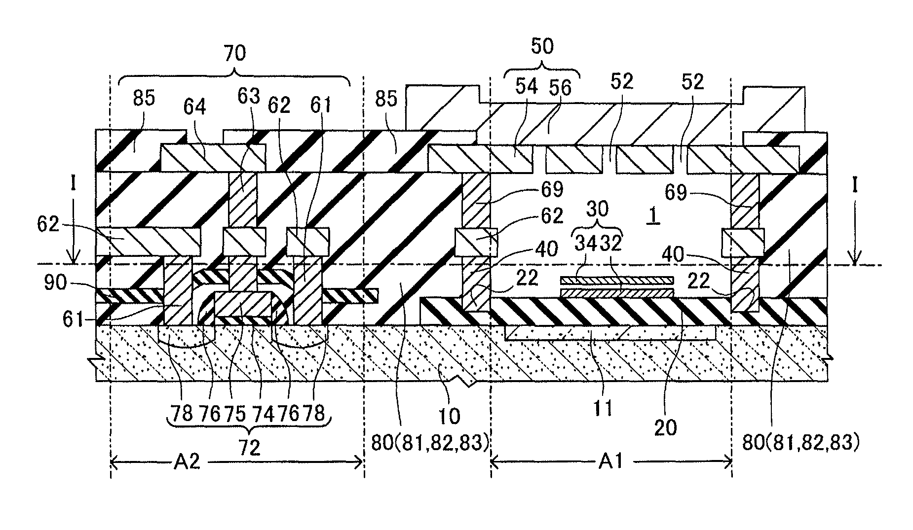
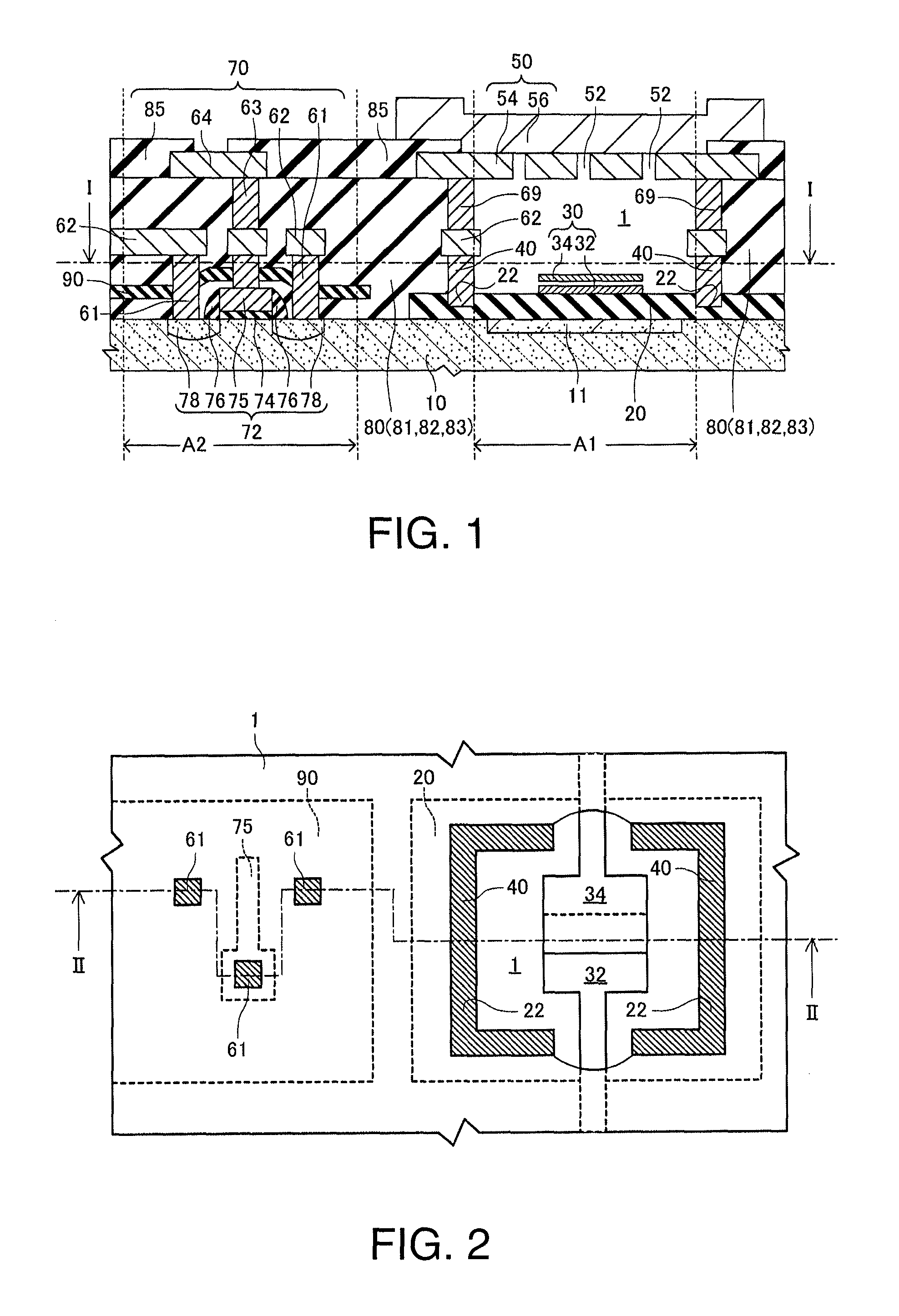
[0051]An electronic device according to an embodiment of the invention will be described with reference to the drawings. FIG. 1 schematically shows a cross section of an electronic device 100 according to the present embodiment. FIG. 2 is a cross-sectional view schematically showing the electronic device 100 according to the present embodiment. FIG. 1 corresponds to a cross section taken along the line II-II in FIG. 2. FIG. 2 corresponds to a cross section taken along the line I...
PUM
| Property | Measurement | Unit |
|---|---|---|
| thickness | aaaaa | aaaaa |
| thickness | aaaaa | aaaaa |
| thickness | aaaaa | aaaaa |
Abstract
Description
Claims
Application Information