Array substrate and liquid crystal display panel

a liquid crystal display panel and array substrate technology, applied in the field of array substrates and liquid crystal display panels, can solve the problems of increasing the degree of scan signal decrease and the gradual decrease of scan signals, and achieve the effect of improving the uniformity of image brightness

Active Publication Date: 2015-12-22
SHENZHEN CHINA STAR OPTOELECTRONICS TECH CO LTD
View PDF1 Cites 4 Cited by
  • Summary
  • Abstract
  • Description
  • Claims
  • Application Information

AI Technical Summary

Benefits of technology

[0021]Beneficial effects can be achieved by the present invention are that: compared with the prior art, in the array substrate of the present invention, by setting the thin film transistors corresponding to different positions of a scan line to have different width-to-length ratios, a voltage difference between the pixel electrodes corresponding to the different positions of the scan line is smaller than a threshold value, and thereby voltages of the pixel electrodes corresponding to the different positions are substantially equal to each other. As a result, brightnesses of display image corresponding to the different positions of the scan line are substantially the same, and the uniformity of image brightness is improved.

Problems solved by technology

However, since the RC delay of signals on the scan line, waveforms of the scan signals inputted to the scan line are distorted, i.e., when the scan signals with original normal waveforms inputted from the two ends of the scan line are transmitted toward the middle of the scan line, suffering from the RC delay influence of the scan line, the scan signals are gradually decreased, and the degree of decrease of the scan signals is more serious when the scan signals reach the middle of the scan line, so that charging ratios of the pixel electrodes 14 in the middle of the liquid crystal display panel 11 are reduced, and voltages 15 of the pixel electrodes 14 in the middle of the liquid crystal display panel 11 are lower than voltages 16 of the pixel electrodes 14 at two sides of the liquid crystal display panel 11, resulting in that a brightness in the middle of the liquid crystal display panel 11 is lower than brightnesses at the two sides of the liquid crystal display panel 11, i.e., the liquid crystal display panel 11 appears the phenomenon of “two sides being whity”, the brightness uniformity of the liquid crystal display panel 11 is degraded consequently.

Method used


Image

  • Array substrate and liquid crystal display panel
  • Array substrate and liquid crystal display panel
  • Array substrate and liquid crystal display panel

Examples


Embodiment Construction

[0039]In the following, with reference to accompanying drawings of embodiments of the present invention, technical solutions in the embodiments of the present invention will be clearly and completely described. Apparently, the embodiments of the present invention described below only are a part of embodiments of the present invention, but not all embodiments. Based on the described embodiments of the present invention, all other embodiments obtained by ordinary skill in the art without creative effort belong to the scope of protection of the present invention.

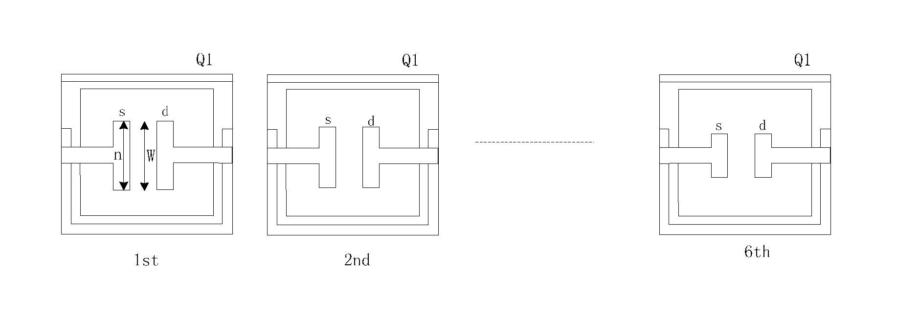
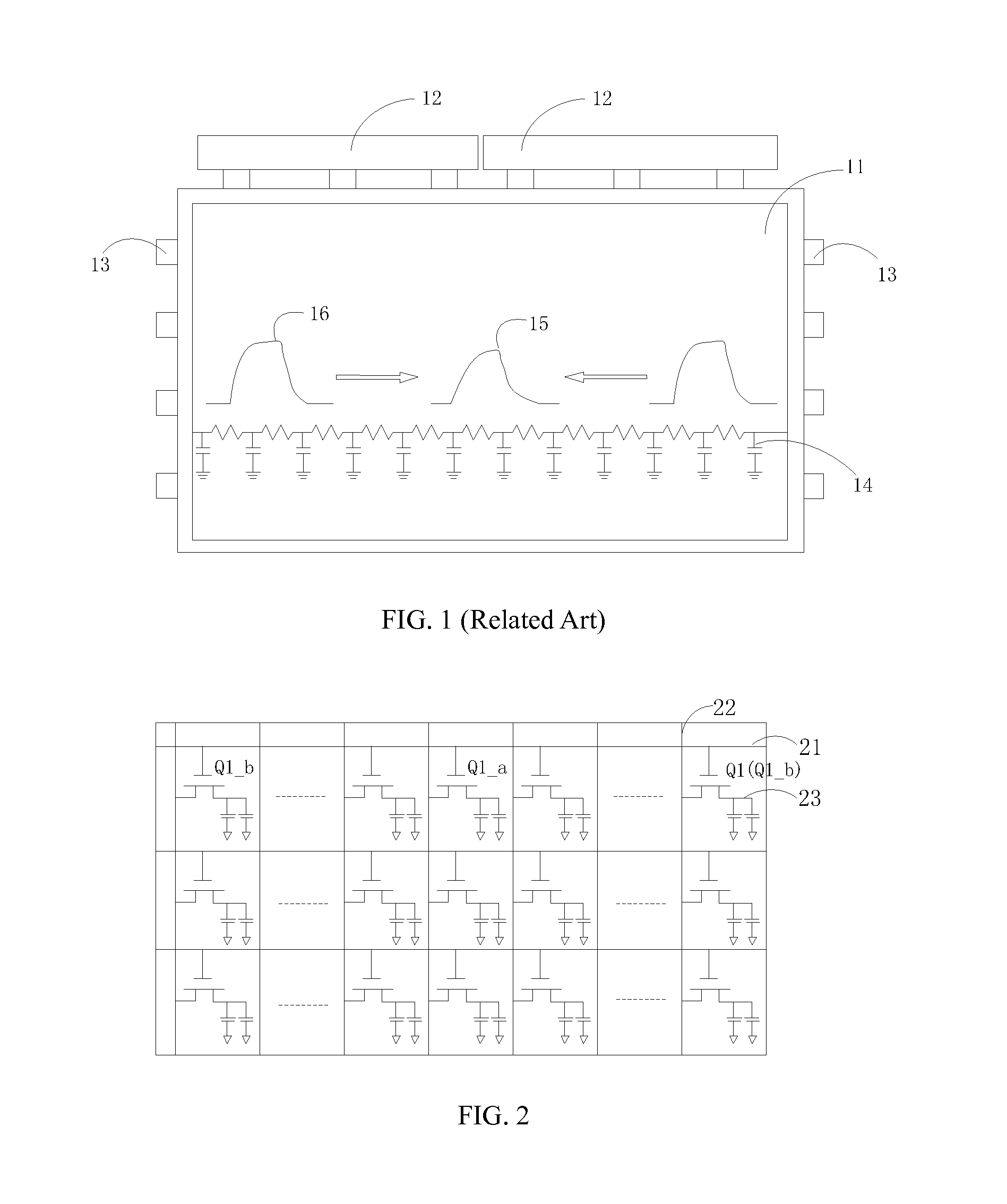
[0040]Referring to FIG. 2, FIG. 2 is an equivalent circuit diagram of pixel structures in an embodiment of an array substrate according to the present invention. The array substrate includes scan lines 21, data lines 22, pixel electrodes 23 and thin film transistors Q1. The scan lines 21 are arranged intersecting with the data lines 22. One pixel electrode 23, one thin film transistor Q1 and mutually intersected one scan line 2...


PUM

PropertyMeasurementUnit
channel widthsaaaaaaaaaa
widthaaaaaaaaaa
widthaaaaaaaaaa

Abstract

The present invention provides an array substrate and a liquid crystal display panel. In the array substrate, as to thin film transistors connected with one scan line, a width-to-length ratio of the thin film transistor(s) corresponding to the middle of the scan line is larger than the width-to-length ratio of the thin film transistors corresponding to two ends of the scan line, and thereby when data lines input voltage signals, a voltage difference between a pixel electrode(s) connected with the thin film transistor(s) corresponding to the middle of the scan line and the pixel electrodes connected with the thin film transistors corresponding to the two ends of the scan line is smaller than a threshold value. By the above described manner, the present invention can improve the uniformity of image brightness.

Description

TECHNICAL FIELD[0001]The present invention relates to the field of liquid crystal display technology, and particularly to an array substrate and a liquid crystal display panel.DESCRIPTION OF RELATED ART[0002]The liquid crystal display panel has advantages of excellent color performance, wide viewing angle, high contrast and so on, and thus has broad market prospects.[0003]As shown in FIG. 1, a liquid crystal display panel 11 generally is driven to display by data drivers 12 and scan drivers 13 arranged at the periphery thereof. Scan signals on one scan line are inputted by the scan drivers 13 respectively connected with two ends of the scan line, so as to control thin film transistors (TFTs) connected with the scan line to be turned on, and then the data drivers 12 can input voltage signals needed by image display to pixel electrodes 14 of the liquid crystal display panel 11 through the turned-on thin film transistors, the display of the liquid crystal display panel 11 is achieved a...

Claims


Application Information

Patent Timeline
Patent Type & Authority Patents(United States)
IPC IPC(8): G02F1/136H01L27/12G02F1/1368G02F1/1362
CPCH01L27/124G02F1/1368G02F1/136227H01L27/1218G02F1/136286H01L29/41733
Inventor ZHENG, HUA
Owner SHENZHEN CHINA STAR OPTOELECTRONICS TECH CO LTD
Why Eureka
Try Eureka