

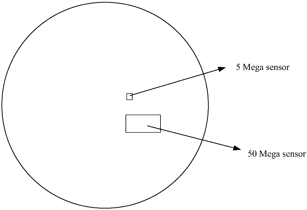
Large-size image sensor and image correction method thereof
An image sensor and image correction technology, applied in the field of image sensors, can solve the problems of large pixel difference, poor image uniformity, pixel difference, etc., to achieve the effect of improving image uniformity
- Summary
- Abstract
- Description
- Claims
- Application Information
AI Technical Summary
Problems solved by technology
Method used
Image

Examples
Embodiment Construction
[0027] In order to make the purpose and features of the present invention more obvious and understandable, the specific implementation of the present invention will be further described below in conjunction with the accompanying drawings. However, the present invention can be implemented in different forms and should not be limited to the described embodiments.
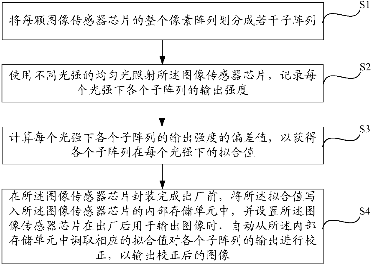
[0028] Please refer to figure 2 , the present invention provides an image correction method for an image sensor, comprising the following steps:
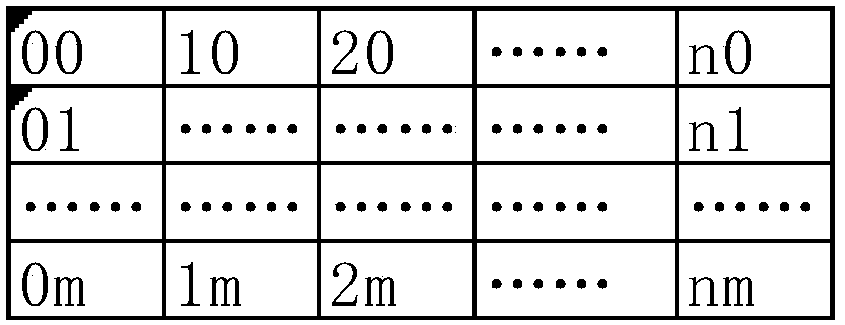
[0029] S1, dividing the entire pixel array of each image sensor chip into several sub-arrays;
[0030] S2, irradiating the image sensor chip with uniform light of different light intensities, and recording the output intensity of each sub-array under each light intensity;
[0031] S3, calculating the deviation value of the output intensity of each sub-array under each light intensity, so as to obtain the fitting value of each sub-array under each light intensity;
[0032...
PUM
 Abstract
Description
Claims
Application Information