Switching power supply circuit
a power supply circuit and switching technology, applied in the direction of power conversion systems, dc-dc conversion, instruments, etc., can solve the problem of low response speed, achieve the effect of improving the response speed to load variation and ensuring the phase margin
- Summary
- Abstract
- Description
- Claims
- Application Information
AI Technical Summary
Benefits of technology
Problems solved by technology
Method used
Image

Examples
first embodiment
[0031]First, the first embodiment will be described.
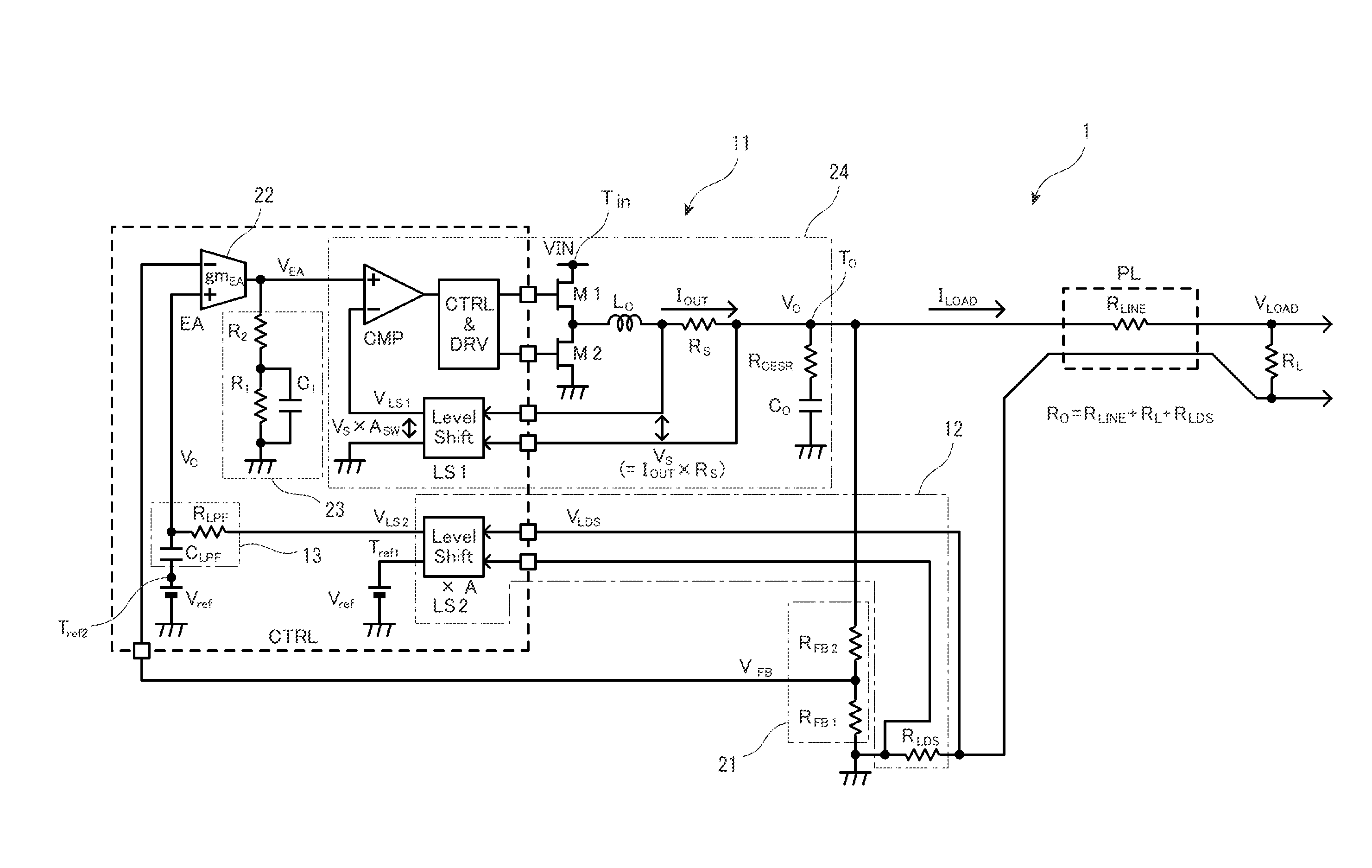
[0032]FIG. 1 is a schematic configuration diagram illustrative of an example of a switching power supply circuit to which the first embodiment of the present invention is applied.
[0033]The switching power supply circuit 1 according to the first embodiment is a current mode DC-DC converter. An output terminal To of the switching power supply circuit 1 is connected to one end of a transmission line PL, and one end of a load RL is connected to the other end of the transmission line PL. The other end of the load RL is connected to a ground line inside the transmission line PL.
[0034]The switching power supply circuit 1 includes: a voltage conversion unit 11 for outputting an output voltage Vo in accordance with an input voltage VIN to the transmission line PL; a signal generation unit 12 for generating a signal in accordance with a voltage that drops in the transmission line PL; and a low pass filter 13 for generating a control signal V...
second embodiment
[0087]Next, the second embodiment of the present invention will be described.
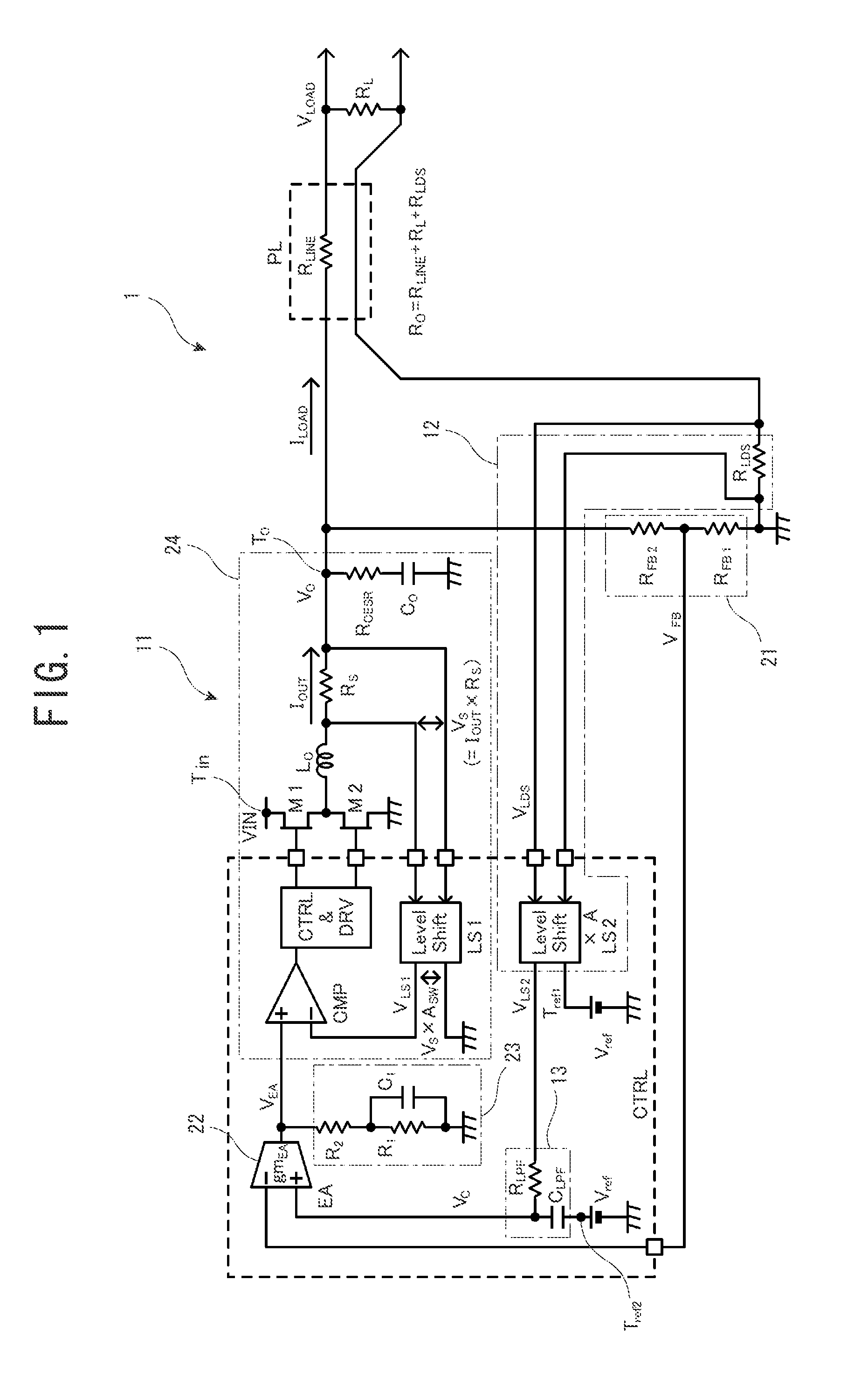
[0088]FIG. 7 is a schematic configuration diagram illustrative of an example of a switching power supply circuit to which the second embodiment of the present invention is applied.
[0089]The switching power supply circuit according to the second embodiment is the same as the switching power supply circuit 1 according to the first embodiment except that the configuration of the signal generation unit 12 is different. Therefore, the same components will be denoted by the same reference signs, and a detailed description thereof will be omitted.
[0090]In the switching power supply circuit 1 of FIG. 1, a signal corresponding to a voltage drop is generated by the sense resistance RLDS arranged between the load RL and the ground and the level shift circuit LS2. On the other hand, as illustrated in FIG. 7, a signal generation unit 12a in a switching power supply circuit 2 according to the second embodiment includes: ...
third embodiment
[0099]Next, the third embodiment of the present invention will be described.
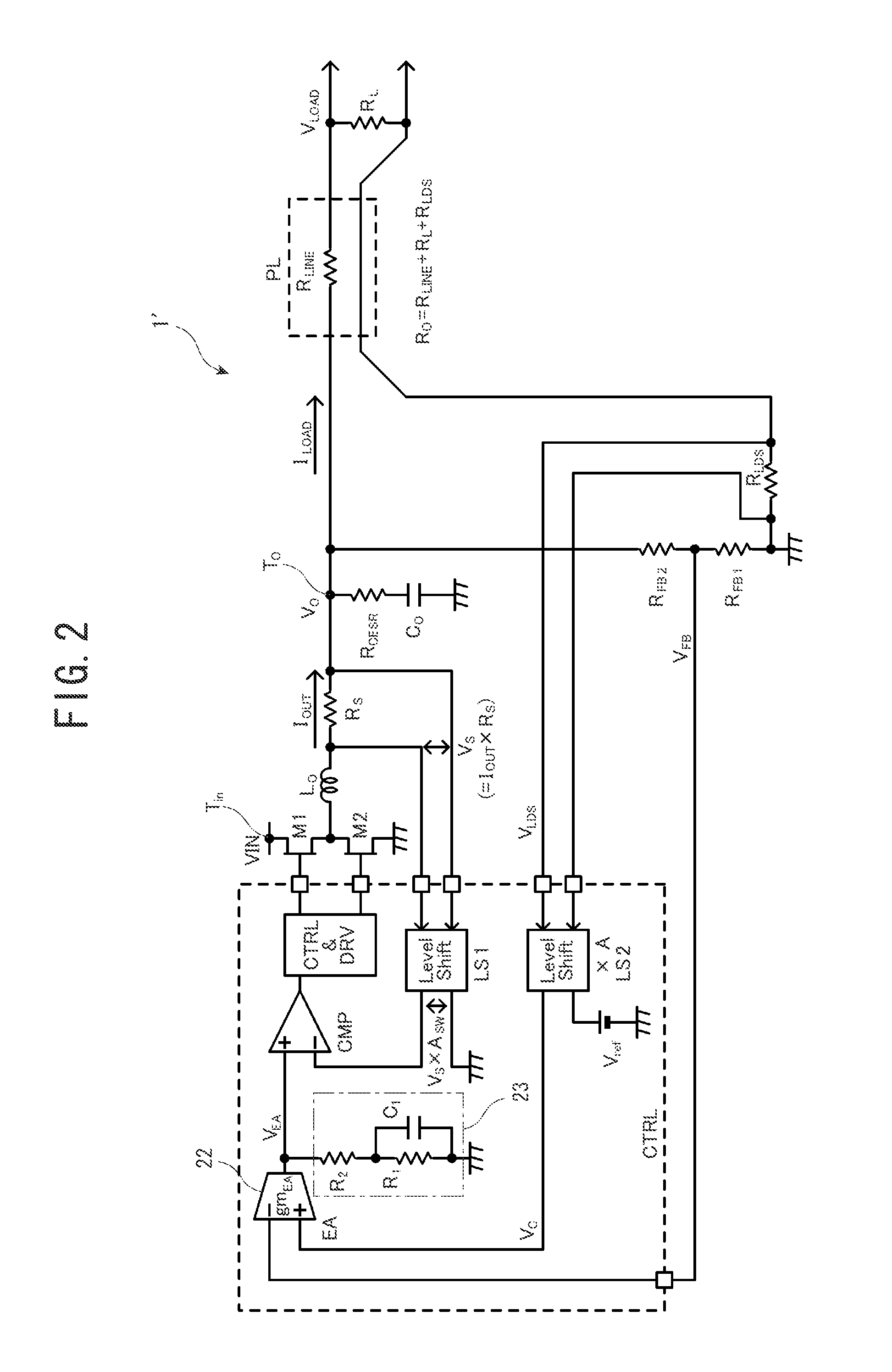
[0100]FIG. 8 is a schematic configuration diagram illustrative of an example of a switching power supply circuit to which the third embodiment of the present invention is applied.
[0101]The switching power supply circuit 3 according to the third embodiment is the same as the switching power supply circuit 2 according to the second embodiment except that the configurations of the signal generation unit 12a and the low pass filter 13 are different. Therefore, the same components will be denoted by the same reference signs, and a detailed description thereof will be omitted.
[0102]A signal generation unit 12b of the switching power supply circuit 3 according to the third embodiment includes: a sense resistance Rs arranged between an inductor Lo and an output terminal To; and a transconductance amplifier gmLD. A low pass filter 13a includes a resistance RLD and a capacitance CLD arranged in parallel to each other ...
PUM
 Abstract
Description
Claims
Application Information