Check patentability & draft patents in minutes with Patsnap Eureka AI!

Methods and apparatus for debugging lowest power states in System-On-Chips

a technology of system-on-chip and lowest power state, which is applied in the direction of power supply for data processing, liquid/fluent solid measurement, instruments, etc., can solve the problems of complex fsms that are prone to errors/bugs in their design, portable electronic devices that consume more battery power,

Active Publication Date: 2016-01-05
NVIDIA CORP
View PDF10 Cites 2 Cited by
  • Summary
  • Abstract
  • Description
  • Claims
  • Application Information

AI Technical Summary

Benefits of technology

The patent describes a method for debugging systems-on-chips (SOCs) that use finite state machines (FSMs) to sequence through different power states. The method involves using a debug logic circuit that is connected to the SOC's voltage source. The voltage sources are turned off in the lowest power states, and the FSMs move from one low power state to the next, generating output signals. These signals are then masked to prevent them from entering low power or reset states. This allows the debug logic circuit to remain powered up and allows for debugging of the lowest power of the SOC. The technical effect of this method is that it enables efficient debugging of complex SOCs that use FSMs and low power states.

Problems solved by technology

Consequently, portable electronic devices consume more battery power.
Generally, with multiple power domains, the sequencing of low power states becomes increasingly difficult, which requires complex power sequencing FSMs implemented in the AO domain.
These complex FSMs are prone to errors / bugs in their design.
However, adding debug logic circuitry on AO rails increases area which increases leakage power and is hence undesirable.
Even if some minor / simple logic is added to AO rails, it fails to provide sufficient visibility for complex debugs of the power sequencing FSMs.

Method used


Image

  • Methods and apparatus for debugging lowest power states in System-On-Chips
  • Methods and apparatus for debugging lowest power states in System-On-Chips
  • Methods and apparatus for debugging lowest power states in System-On-Chips

Examples


Embodiment Construction

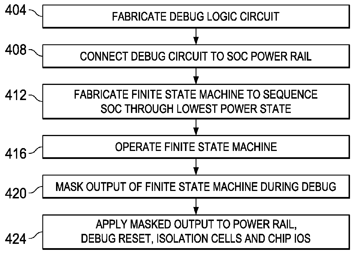
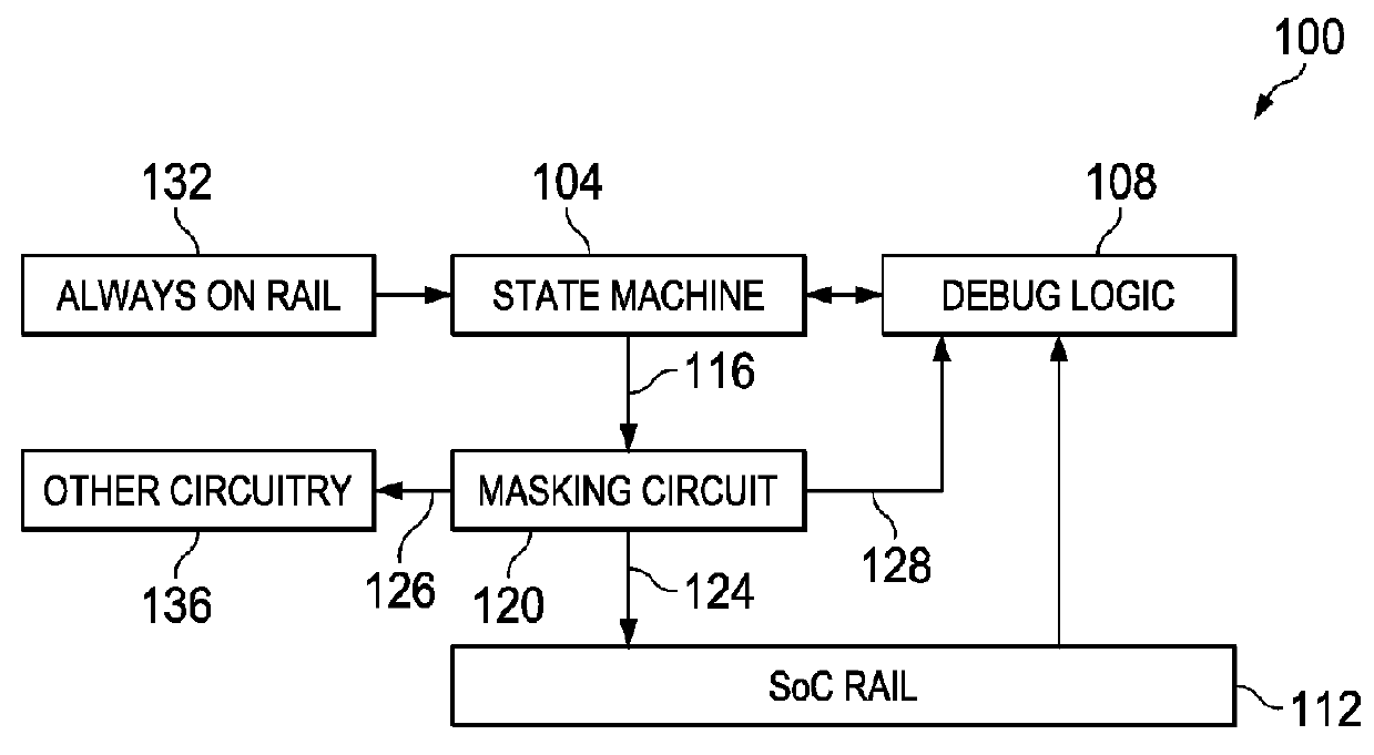
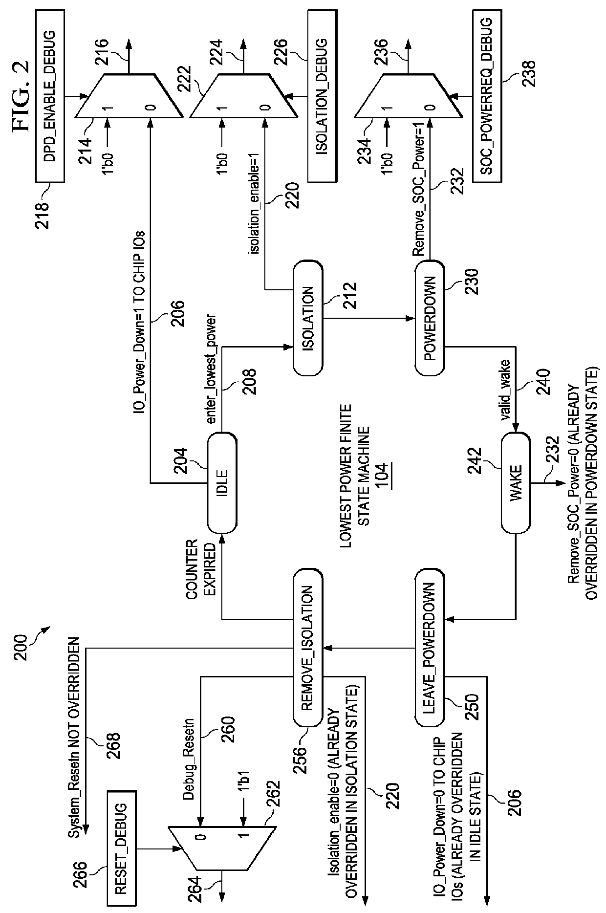
[0014]It is realized herein that a need exists for methods and apparatus for debugging finite state machines (FSMs) that sequence the System-On-Chips (SOCs) through the lowest power states where only the AO power rail is turned ON while other rails are turned off.

[0015]FIGS. 1-4, discussed below, and the various embodiments used to describe the principles of the present disclosure are by way of illustration only and should not be construed in any way to limit the scope of the disclosure. Those skilled in the art will recognize that the principles of the disclosure may be implemented in any suitably arranged device or a system. The numerous innovative teachings of the present disclosure will be described with reference to exemplary non-limiting embodiments.

[0016]Various disclosed embodiments are directed to apparatus and method for debugging FSMs that sequence the SOC through a plurality of low power states. According to certain disclosed embodiments, a finite state machine in AO pow...


PUM


Abstract

Methods and apparatus for debugging finite state machine are disclosed. The method includes implementing a debug logic circuit and connecting the debug logic circuit to a system on chip (SoC) voltage source. The method includes operating a finite state machine that sequences the SoC from a low power state to a next low power state and generating respective output signals corresponding to the low power states and wherein the finite state machine is connected to Always On voltage source. The method includes masking the output signals to generate respective masked output signals, and applying the masked output signals to SoC circuit elements to prevent from transitioning into low power states and hence keeping the debug logic circuitry alive. The method includes debugging the finite state machine in the lowest power state by the debug logic circuit.

Description

TECHNICAL FIELD[0001]The present disclosure is directed, to methods and apparatus for debugging lowest power states in System-On-Chips.BACKGROUND[0002]Mobile phones, tablets and other portable electronic devices continue to offer higher performance and more features. Consequently, portable electronic devices consume more battery power. To prolong battery life without sacrificing performance or features, it is desirable to minimize active and leakage power consumption in portable devices.[0003]In most portable devices, one or more System-On-Chips (SoCs) are implemented to perform various functions. During operation, SoCs may group or segregate logic circuitry into power domains that can be independently powered OFF when not in use. By grouping the logic circuitry into power domains, the logic circuitry may be sequenced through multiple low power states. Generally, one or more Finite State Machines (FSMs) are utilized for sequencing logic circuitry through various low power states. A ...

Claims


Application Information

Patent Timeline
Patent Type & Authority Patents(United States)
IPC IPC(8): G01R31/317G06F1/32G06F1/26
CPCG01R31/31705G01R31/31721G06F1/26G06F1/266G06F1/3203G06F1/3206G06F1/329G06F1/3228G06F1/3243
Inventor KRISHNANI, PADAMAGRAWAL, SUPREETNG, KWANJEE
Owner NVIDIA CORP
Features
  • R&D
  • Intellectual Property
  • Life Sciences
  • Materials
  • Tech Scout
  • Unparalleled Data Quality
  • Higher Quality Content
  • 60% Fewer Hallucinations
Learn More