Semiconductor devices and methods of manufacturing the same

a technology of semiconductors and semiconductors, applied in the direction of semiconductor devices, basic electric elements, electrical equipment, etc., can solve the problems of reduced quantum efficiency, relatively complex processes associated with these alternatives, and limited internal quantum efficiency of nitride thin films, so as to suppress the bending stress of substrates, reduce the defect density of thin films, and improve light extraction efficiency

Active Publication Date: 2016-01-05
SAMSUNG ELECTRONICS CO LTD +1
View PDF22 Cites 0 Cited by
  • Summary
  • Abstract
  • Description
  • Claims
  • Application Information

AI Technical Summary

Benefits of technology

[0012]Semiconductor devices, and methods of manufacturing the same, according to at least some example embodiments also have reduced defect density of the thin film and / or suppressed bending stresses of the substrate and the thin film.
[0013]Example embodiments also provide semiconductor devices having improved light extraction efficiency, and methods of manufacturing the same.

Problems solved by technology

Thus, an internal quantum efficiency of the nitride thin film is relatively limited.
These defects function as non-emission portions and cause a reduction in quantum efficiency.
However, processes associated with these alternatives are relatively complex, which increases costs and time.

Method used


Image

  • Semiconductor devices and methods of manufacturing the same
  • Semiconductor devices and methods of manufacturing the same
  • Semiconductor devices and methods of manufacturing the same

Examples


Embodiment Construction

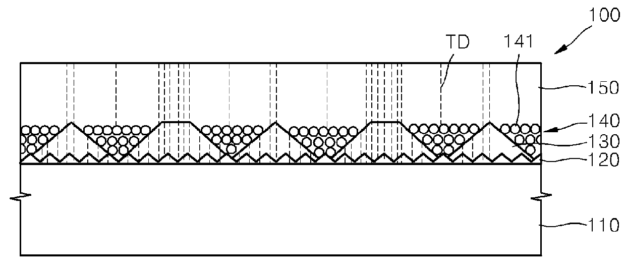
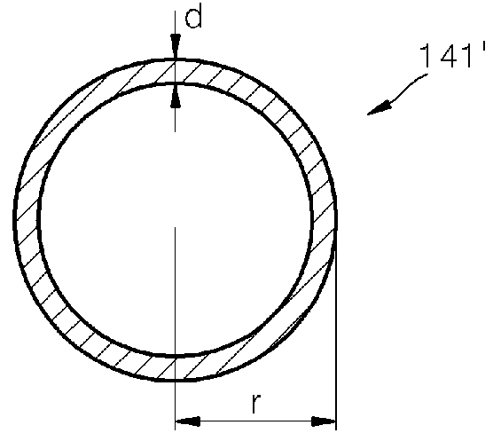
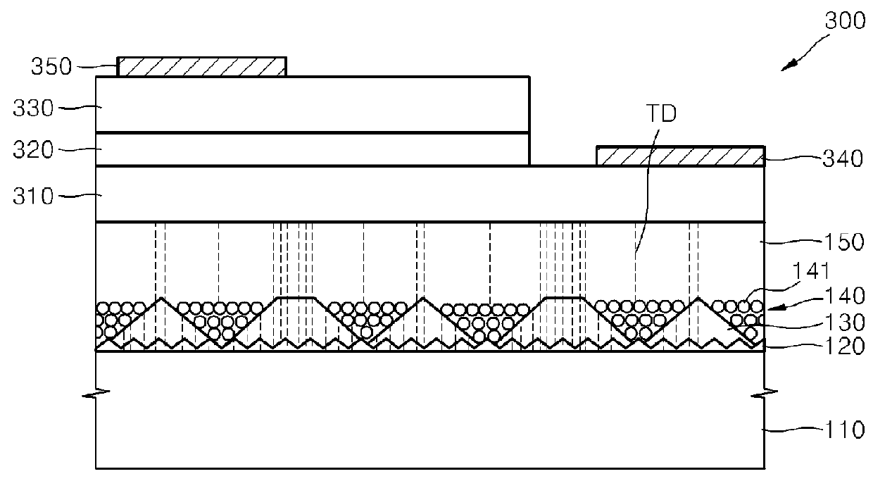
[0044]Example embodiments will now be described more fully with reference to the accompanying drawings, in which some example embodiments are shown. In the drawings, the thicknesses of layers and regions are exaggerated for clarity. Like reference numerals in the drawings denote like elements.

[0045]Detailed illustrative embodiments are disclosed herein. However, specific structural and functional details disclosed herein are merely representative for purposes of describing example embodiments. Example embodiments may be embodied in many alternate forms and should not be construed as limited to only those set forth herein.

[0046]It should be understood, however, that there is no intent to limit this disclosure to the particular example embodiments disclosed. On the contrary, example embodiments are to cover all modifications, equivalents, and alternatives falling within the scope of the invention. Like numbers refer to like elements throughout the description of the figures.

[0047]It w...


PUM


Abstract

A semiconductor device includes a first non-flat non-polar nitride semiconductor layer, a first structure layer on at least a portion of the surface of the first non-flat non-polar nitride semiconductor layer and a first non-polar nitride semiconductor layer on the first non-flat non-polar nitride semiconductor layer and the first structure layer. The first non-flat non-polar nitride semiconductor layer includes a plurality of solid particles.

Description

CROSS-REFERENCE TO RELATED APPLICATION(S)[0001]This application claims priority under 35 U.S.C. §119 to Korean Patent Application No. 10-2011-0012863, filed on Feb. 14, 2011, in the Korean Intellectual Property Office, the disclosure of which is incorporated herein in its entirety by reference.BACKGROUND[0002]1. Field[0003]Example embodiments relate to semiconductor devices including a non-polar face, and / or methods of manufacturing the same.[0004]2. Description of the Related Art[0005]A semiconductor material grown in a heterojunction semiconductor thin film structure may be used to form optical or electrical devices by adjusting a lattice constant or a band gap of the semiconductor. A nitride semiconductor is an example of such a semiconductor material.[0006]A nitride semiconductor is relatively stable both thermally and chemically, and also has a relatively wide direct transition band gap. Thus, a nitride semiconductor material is used to form electronic devices, such as heteroju...

Claims


Application Information

Patent Timeline
Patent Type & Authority Patents(United States)
IPC IPC(8): H01L29/778H01L21/02
CPCH01L21/0254H01L21/0242H01L21/02378H01L21/02381H01L21/02392H01L21/02395H01L21/02398H01L21/02488H01L21/02628H01L21/02647H01L21/02458H01L21/02494H01L21/02513H01L21/02642H01L33/0075
Inventor LEE, SANGMOONYOON, EUIJOONPARK, JINSUBPARK, SUNG HYUN
Owner SAMSUNG ELECTRONICS CO LTD
Why Eureka
Try Eureka