Liquid crystal display device and fabricating method thereof

a technology of liquid crystal display and fabrication method, which is applied in the direction of instruments, non-linear optics, optics, etc., can solve the problems of deterioration such as light leakage, and the characteristics of tft become non-uniform, so as to achieve the effect of preventing photocurrent generation, improving aperture ratio, and improving the operating characteristic of thin film transistors

Active Publication Date: 2016-03-01
LG DISPLAY CO LTD
View PDF6 Cites 9 Cited by
  • Summary
  • Abstract
  • Description
  • Claims
  • Application Information

AI Technical Summary

Benefits of technology

[0015]An object of the present invention is to provide a liquid crystal display device and a fabricating method thereof in which a photocurrent generation is effectively prevented and an aperture ratio is...

Problems solved by technology

When attaching the array substrate and the color filter substrate, deterioration such as light leakage may occur due to misalignment.
However, since the black matrix is spaced apart ...

Method used


Image

  • Liquid crystal display device and fabricating method thereof
  • Liquid crystal display device and fabricating method thereof
  • Liquid crystal display device and fabricating method thereof

Examples


first embodiment

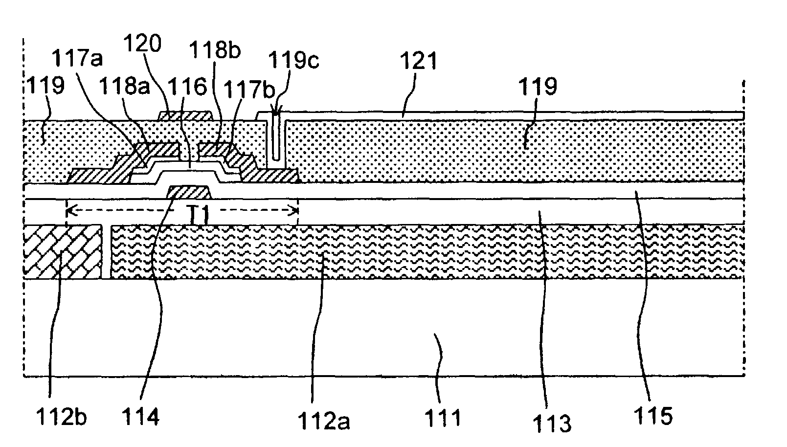
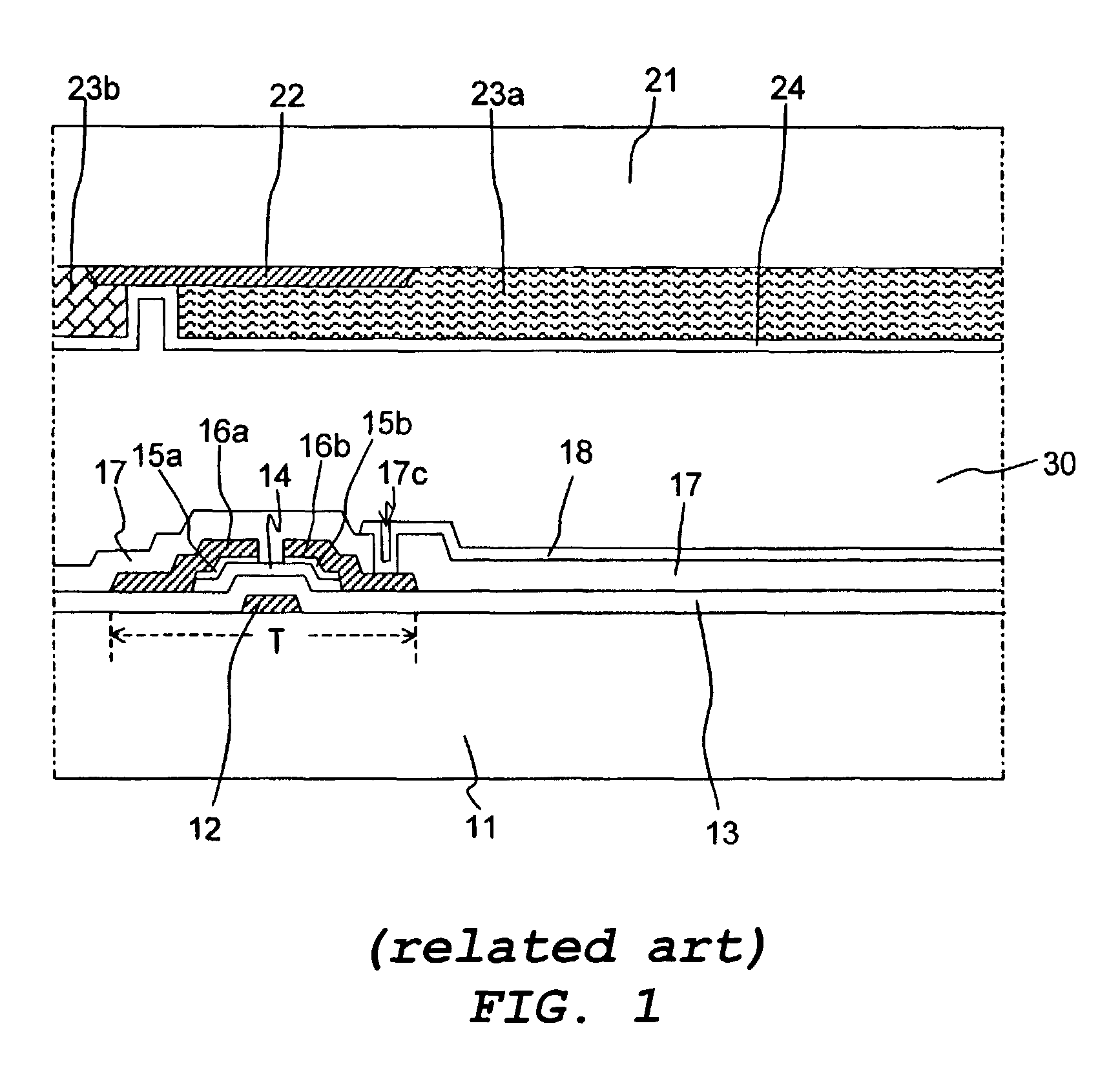
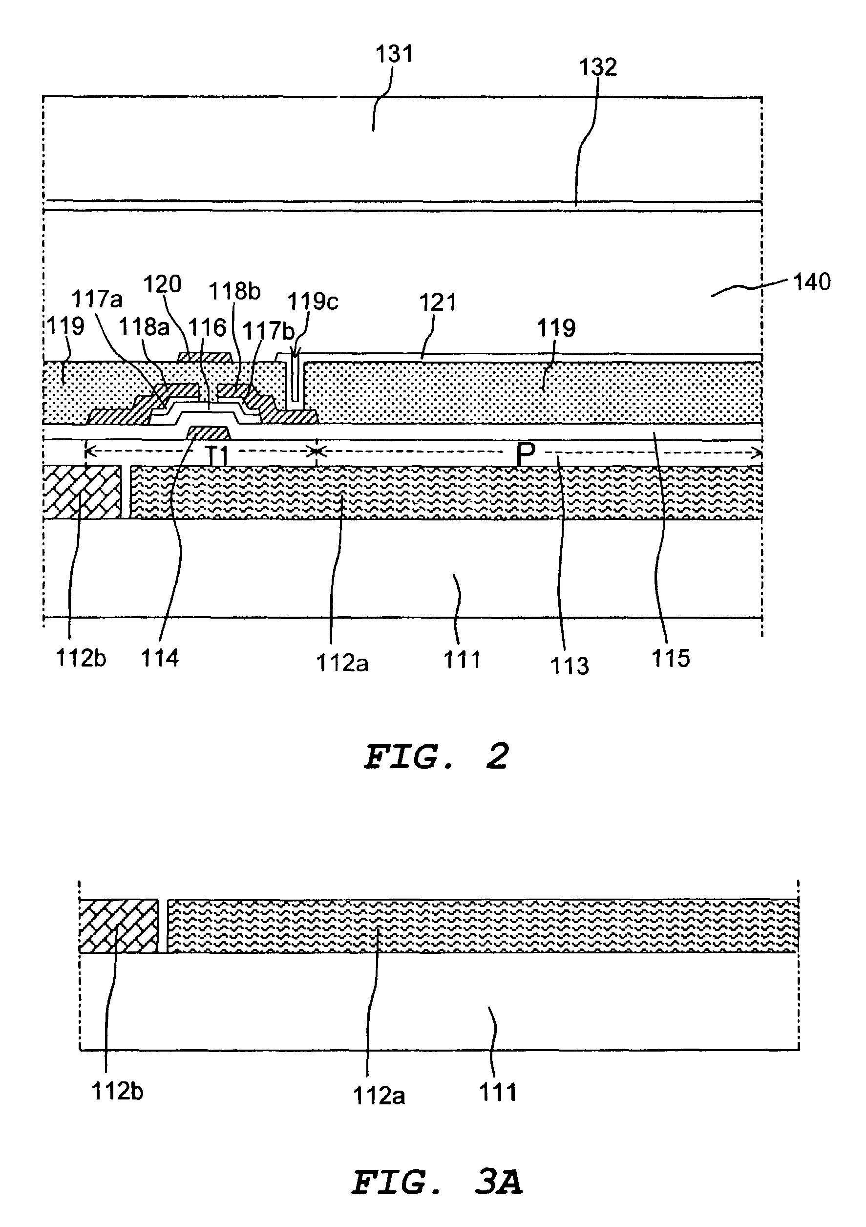
[0034]FIG. 2 is a schematic cross-sectional view of a liquid crystal display device according to the present invention. The LCD device of FIG. 2 has a TOC type structure in which a color filter layer is formed under a TFT.

[0035]In FIG. 2, a first substrate 111 and a second substrate 131 are facing into and spaced apart from each other. A color filter layer 112a and 112b is formed on the inner surface of the first substrate 111. The color filter layer 112a and 112b having three colors of R, G, and B is alternately disposed. An overcoat layer 113 is formed on the color filter layer 112a and 112b. The overcoat layer 113 protects the color filter layer112a and 112b and planarizes the top surface of the color filter layer 112a and 112b to stabilize the following processes.

[0036]A gate electrode 114 of a conductive material such as metal is formed on the overcoat layer 113 and a gate insulating layer 115 covers the gate electrode 114. The gate electrode 114 is connected to a gate line (no...

second embodiment

[0049]FIG. 4 is a schematic cross-sectional view of a liquid crystal display device according to the present invention. The LCD device of FIG. 2 has a COT type structure in which a color filter layer is formed over a TFT.

[0050]In FIG. 4, a first substrate 211 and a second substrate 221 are facing into and spaced apart from each other. A gate electrode 212 of a conductive material such as metal is formed on the inner surface of the first substrate 211 and a gate insulating layer 213 covers the gate electrode 212. The gate electrode 212 is connected to a gate line (not shown). An active layer 214 of amorphous silicon is formed on the gate insulating layer 213 over the gate electrode 212. An ohmic contact layer 215a and 215b of impurity-doped amorphous silicon is formed on the active layer 214. Source and drain electrodes 216a and 216b forming a TFT “T2” with the gate electrode 212 are formed on the ohmic contact layer 215a and 215b. The source electrode 216a is connected to a data lin...


PUM


Abstract

A liquid crystal display device includes first and second substrates facing into each other, a gate line and a data line on an inner surface of the first substrate, the gate line and the data line defining a pixel region, a thin film transistor connected to the gate line and the data line, a pixel electrode connected to the thin film transistor and disposed at the pixel region, a color filter layer disposed closer than the pixel electrode from the first substrate, the color filter layer corresponding to the pixel electrode, a black matrix over the thin film transistor, a common electrode on an inner surface of the second substrate, and a liquid crystal layer interposed between the pixel electrode and the common electrode.

Description

[0001]This application claims the benefit of the Korean Patent Application No. P2001-44757 filed on Jul. 25, 2001, which is hereby incorporated by reference.BACKGROUND OF THE INVENTION[0002]1. Field of the Invention[0003]The present invention relates to a liquid crystal display, and more particularly, to a liquid crystal display device and a fabricating method thereof. Although the present invention is suitable for a wide scope of applications, it is particularly suitable for preventing a photocurrent generation and improving an aperture ratio of the liquid crystal display device.[0004]2. Discussion of the Related Art[0005]Flat panel display (FPD) devices having small size, lightweight, and low power consumption may have been a subject of recent research in the advent of the information age. Among many kinds of FPD devices, liquid crystal display (LCD) devices have been widely developed and used because of their excellent characteristics in resolution, color display, and display qua...

Claims


Application Information

Patent Timeline
IPC IPC(8): G02F1/1362G02F1/1335
CPCG02F1/136209G02F2001/136222G02F2201/40G02F1/136222G02F1/1335
Inventor CHANG, YOUN-GYOUNGKIM, WOONG-KWON
Owner LG DISPLAY CO LTD
Why Eureka
Try Eureka