Dielectric ceramic, multi-layer ceramic capacitor and method of manufacturing the same

a multi-layer ceramic and capacitor technology, applied in the direction of fixed capacitors, basic electric elements, electrical equipment, etc., can solve the problems of the dielectric constant to drop, suppress the generation of oxygen defects, suppress the growth of grains, and reduce the quantity of oxygen

Active Publication Date: 2016-03-08
TAIYO YUDEN KK
View PDF13 Cites 7 Cited by
  • Summary
  • Abstract
  • Description
  • Claims
  • Application Information

AI Technical Summary

Benefits of technology

[0009]However, adding Mn or other acceptor element to a complex oxide of BaTiO3, for example, leads to sintering in a solid solution state where some of the Ti sites of the crystal lattice in the shell of crystal grains are substituted by Mn. In this case, the greater the quantity of acceptor element added, the more the generation of oxygen defects is suppressed. In the meantime, the probability also increases that the lattice constant and orientation vary according to the Mn-substituted quantity and substitution position in the crystal shells contacting each other, consequently suppressing the grain growth due to sintering. In other words, adding a larger quantity of acceptor element with the aim of reducing the quantity of oxygen defects reduces the grain size of dielectric crystal and the resulting sizing effect causes the dielectric constant to drop, which presents a problem.
[0017]Furthermore, the present invention provides a method of manufacturing a dielectric ceramic including: a step to sinter a dielectric in a reducing ambience where the primary component of the dielectric is ABO3 (A represents an element containing Ba, while B represents an element containing Ti), an acceptor element is contained by p mol per 100 mol of ABO3 and the letter p representing the mol number of the acceptor element is in a range of 0<p≦0.5; and a step to oxidize the sintered dielectric in an oxidizing ambience to reduce the oxygen defect concentration of the sintered grains constituting the dielectric.
[0021]Moreover, the present invention provides a method of manufacturing a multi-layer ceramic capacitor including: a step to prepare a dielectric green sheet whose primary component is ABO3 (A represents an element containing Ba, while B represents an element containing Ti) and which contains an acceptor element by no more than 0.5 mol per 100 mol of ABO3; a step to print a conductive paste on the dielectric green sheet to provide an internal electrode layer; a step to stack the dielectric green sheets on which the conductive paste has been printed, to form a capacitor laminate; a step to sinter the capacitor laminate in a reducing ambience; and a step to oxidize the sintered capacitor laminate in an oxidizing ambience to reduce the oxygen defect concentration of the sintered grains constituting the dielectric layer in the capacitor laminate.
[0025]According to the present invention, the oxygen defect concentration in the dielectric can be reduced and a sufficient dielectric constant can also be ensured.

Problems solved by technology

In other words, adding a larger quantity of acceptor element with the aim of reducing the quantity of oxygen defects reduces the grain size of dielectric crystal and the resulting sizing effect causes the dielectric constant to drop, which presents a problem.

Method used


Image

  • Dielectric ceramic, multi-layer ceramic capacitor and method of manufacturing the same
  • Dielectric ceramic, multi-layer ceramic capacitor and method of manufacturing the same
  • Dielectric ceramic, multi-layer ceramic capacitor and method of manufacturing the same

Examples


example

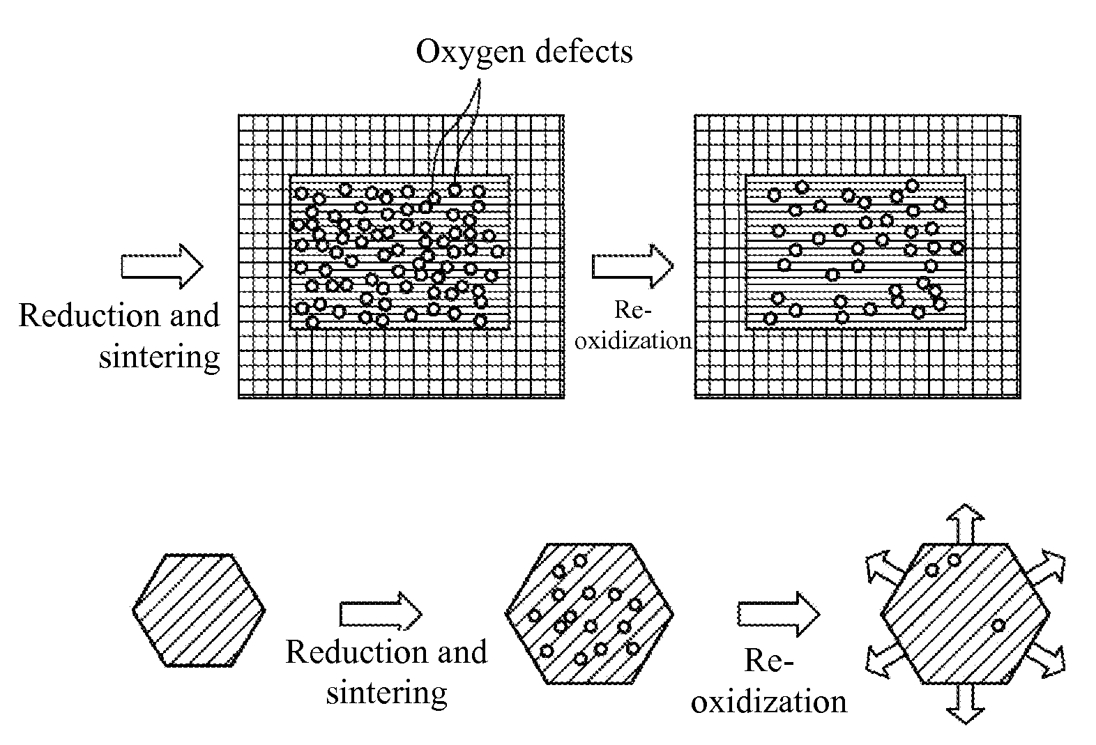
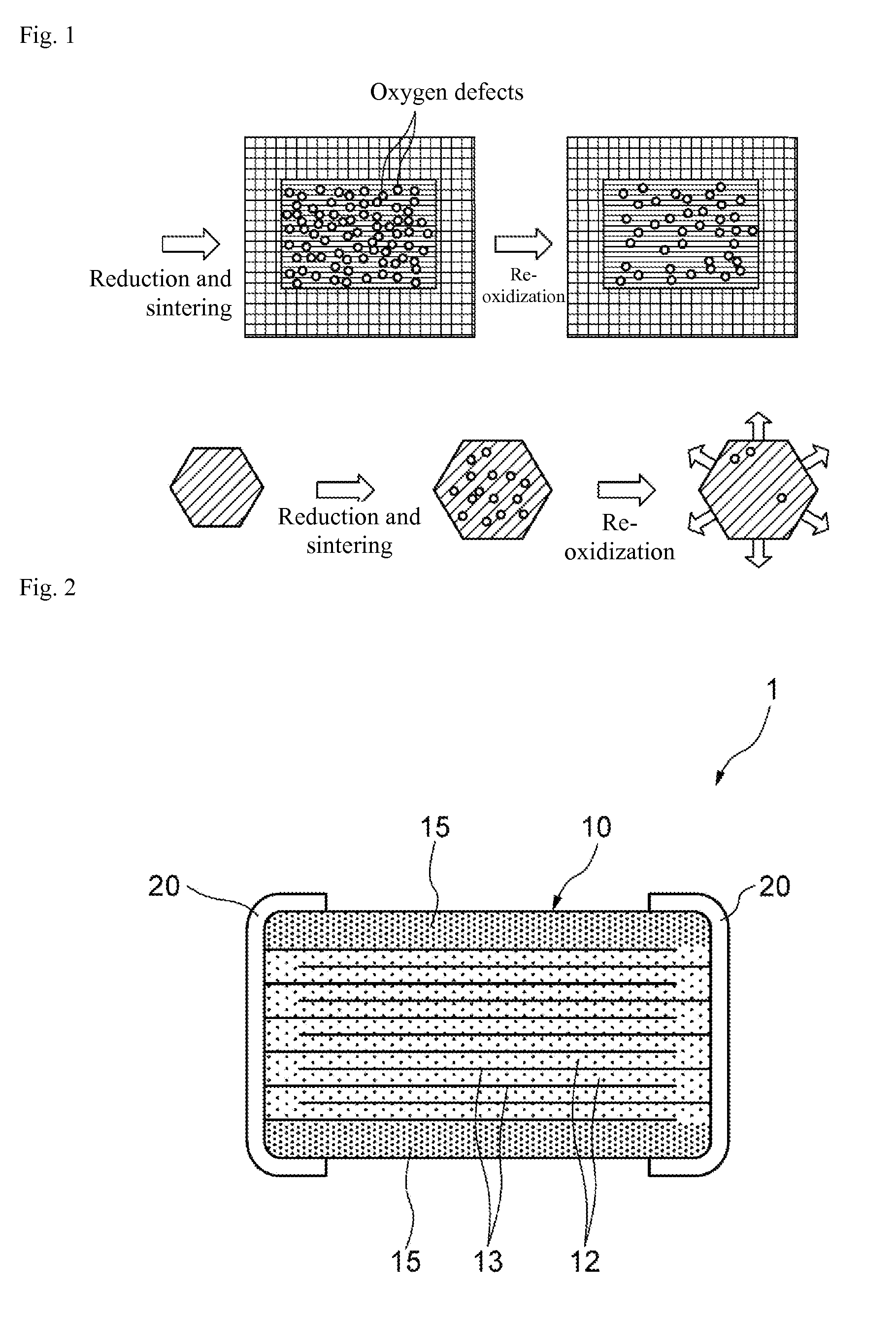
[0044]Next, an example of a multi-layer ceramic capacitor is explained, where dielectric layers to which a dielectric ceramic (MLCC) having such characteristics is applied are stacked at high density. FIG. 2 is a longitudinal section view showing a rough structure of a prototype multi-layer ceramic capacitor 1. The multi-layer ceramic capacitor 1 comprises a sintered compact 10 having chip dimensions and shape specified by the standard (such as a rectangular solid of 1.0 mm×0.5 mm×0.5 mm) and a pair of external electrodes 20, 20 formed on both sides of the sintered compact 10. The sintered compact 10 is comprised of many dielectric layers 12 constituted by dielectric ceramics stacked alternately with many internal electrode layers 13 (there are 100 layers in the example), and cover layers 15 are formed as the outermost layers of the foregoing. The dielectric layers 12 and cover layers 15 contain BaTiO3 (hereinafter referred to as “BT”) as the primary component, while the internal el...


PUM

PropertyMeasurementUnit
grain sizeaaaaaaaaaa
temperatureaaaaaaaaaa
thicknessaaaaaaaaaa

Abstract

A dielectric ceramic is formed with sintered grains constituting the dielectric have an average grain size of 0.2 to 1.0 μm and an oxygen defect concentration of 0.2 to 0.5%. An acceptor element is added to the dielectric ceramic by no more than 0.5 mol per 100 mol of the primary component of BaTiO3. The oxygen defect concentration is temporarily increased by reduction and sintering, after which the oxygen defect concentration is reduced through the subsequent re-oxidization process. Crystal strain generated in the re-oxidization process increases the dielectric constant.

Description

FIELD OF THE INVENTION[0001]The present invention relates to a dielectric ceramic, and a multi-layer ceramic capacitor comprising a laminate of dielectric layers constituted by a dielectric ceramic, as well as method of manufacturing the dielectric ceramic and multi-layer ceramic capacitor of high dielectric constant.DESCRIPTION OF THE RELATED ART[0002]As mobile phones and other digital electronic devices are becoming increasingly smaller and thinner, multi-layer ceramic capacitors (MLCCs) that are surface-mounted on electronic circuit boards, etc., are also becoming smaller. According to the trend for smaller chips, the need for larger-capacity multi-layer ceramic capacitors has been increasing every year. Multi-layer ceramic capacitors are structured in such a way that dielectric layers constituted by dielectric ceramics are alternately layered with internal electrode layers.[0003]In general, reducing the capacitor size invariably reduces the areas of the electrode layers facing t...

Claims


Application Information

Patent Timeline
Patent Type & Authority Patents(United States)
IPC IPC(8): H01G4/12C04B35/468H01G4/30
CPCH01G4/1218C04B35/4682H01G4/1227H01G4/30C04B2235/3206C04B2235/3217C04B2235/3224C04B2235/3236C04B2235/3239C04B2235/3241C04B2235/3262C04B2235/3272C04B2235/3275C04B2235/3279C04B2235/3281C04B2235/3284C04B2235/5445C04B2235/652C04B2235/6584C04B2235/663C04B2235/785H01G4/12
Inventor TANIGUCHI, KATSUYASHIMURA, TETSUO
Owner TAIYO YUDEN KK
Why Eureka
Try Eureka