Air gap semiconductor structure with selective cap bilayer

a semiconductor structure and selective cap technology, applied in semiconductor devices, semiconductor/solid-state device details, electrical devices, etc., can solve the problems of poor reliability, increased resistance, and open conductors

Active Publication Date: 2016-04-05
TESSERA INC
View PDF15 Cites 311 Cited by
  • Summary
  • Abstract
  • Description
  • Claims
  • Application Information

AI Technical Summary

Benefits of technology

[0005]According to one embodiment of the present invention, a semiconductor structure is provided, the semiconductor structure comprising: a dielectric layer present on a semiconductor substrate; one or more conductors within the dielectric layer, wherein the one or more conductors have a top surface; a bilayer cap present on the one or more conductors, wherein the bilayer cap comprises a first layer and a second layer; and a plurality of air gaps, wherein the air gaps are etched into the dielectric layer.
[0006]According to another

Problems solved by technology

Integration processes used in the formation of air gap structures are known in some cases to attack the

Method used


Image

  • Air gap semiconductor structure with selective cap bilayer
  • Air gap semiconductor structure with selective cap bilayer
  • Air gap semiconductor structure with selective cap bilayer

Examples


Embodiment Construction

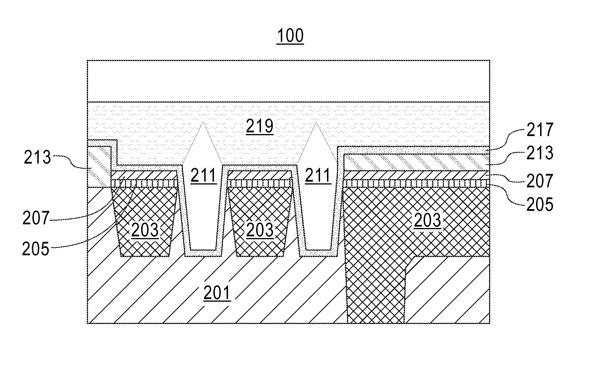
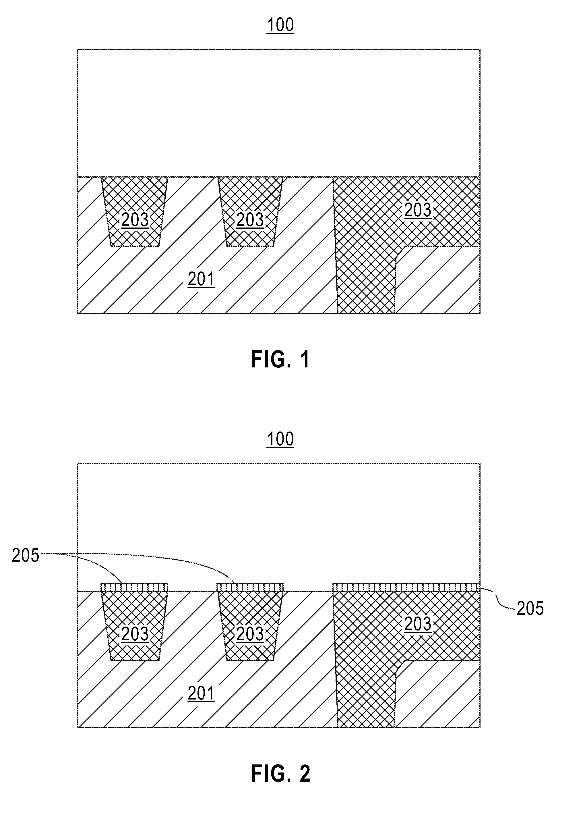
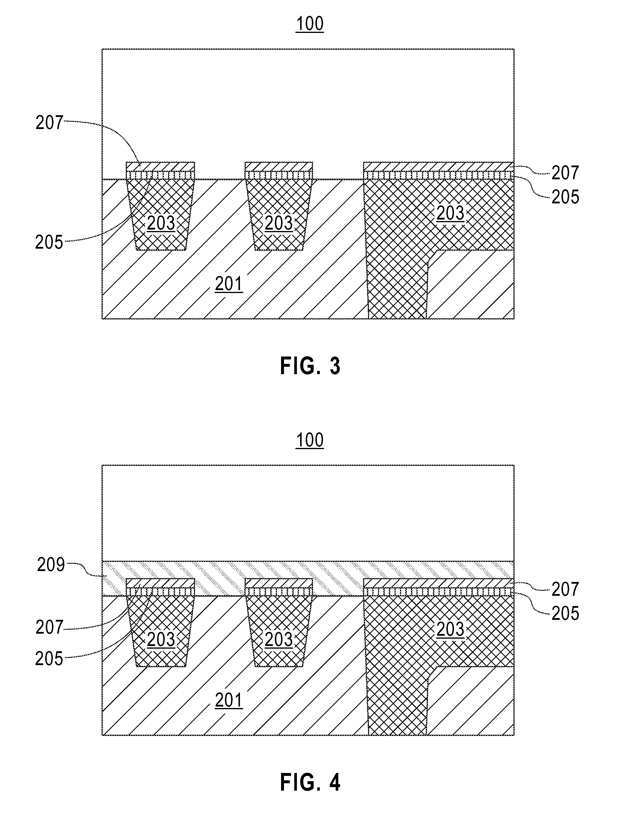
[0016]Embodiments generally provide an air gap structure between metal conductors, including a bilayer self-aligned cap on the metal conductors, used as part of an electronic device structure. Herein, the terms “semiconductor device” and “electronic device” are used to mean an integrated circuit. Embodiments of the present invention provide improved electrical performance in semiconductor devices through power savings and increasing the speed of signal propagation. Detailed description of embodiments of the claimed structures and methods are disclosed herein; however, it is to be understood that the disclosed embodiments are merely illustrative of the claimed structures and methods that may be embodied in various forms. In addition, each of the examples given in connection with the various embodiments is intended to be illustrative, and not restrictive. Further, the figures are not necessarily to scale, some features may be exaggerated to show details of particular components. There...


PUM


Abstract

A semiconductor substrate including one or more conductors is provided. A first layer and a second layer are deposited on the top surface of the conductors. A dielectric cap layer is formed over the semiconductor substrate and air gaps are etched into the dielectric layer. The result is a bilayer cap air gap structure with effective electrical performance.

Description

BACKGROUND OF THE INVENTION[0001]The present invention relates generally to semiconductor devices, and more particularly to the formation of air gap structures in a semiconductor device with a bilayer selective cap.[0002]Semiconductor devices generally include a plurality of circuits which form an integrated circuit fabricated on a semiconductor substrate. To improve the performance of the circuits, low k dielectric materials, having a dielectric constant of less than silicon dioxide, are used between circuits as inter-layer dielectric (ILD) to reduce capacitance. Interconnect structures made of metal lines are usually formed in and around the ILD material to connect elements of the circuits. Within a typical interconnect structure, metal lines run parallel to the semiconductor substrate. An interconnect structure may consist of multilevel or multilayered schemes, such as, single or dual damascene wiring structures.[0003]Manufacture of a semiconductor device, also called an electron...

Claims


Application Information

Patent Timeline
IPC IPC(8): H01L23/48H01L23/532H01L21/311H01L23/528H01L21/768
CPCH01L21/7682H01L23/528H01L23/53223H01L23/53238H01L23/53252H01L23/53266H01L23/53209H01L23/5329H01L21/76802H01L21/7685H01L21/76834H01L21/31111H01L21/28556H01L21/288H01L21/76849H01L21/76856H01L21/76862H01L21/76864H01L23/5222H01L23/53295H01L2924/0002
Inventor GATES, STEPHEN M.HUANG, ELBERT E.KIOUSSIS, DIMITRI R.PENNY, CHRISTOPHER J.PRIYADARSHINI, DEEPIKA
Owner TESSERA INC
Why Eureka
Try Eureka