
Organic electro-luminescent device

a technology of electroluminescent devices and organic semiconductors, applied in the direction of organic semiconductor devices, semiconductor devices, instruments, etc., can solve the problems of deteriorating the light emitting layer, potential display failure, and detection of defects, so as to inhibit the occurrence of lighting failure and suppress manufacturing costs

Active Publication Date: 2016-04-05
JAPAN DISPLAY INC
View PDF18 Cites 2 Cited by
  • Summary
  • Abstract
  • Description
  • Claims
  • Application Information

AI Technical Summary

Benefits of technology

The patent aims to develop a display device that lowers production costs and avoids lighting issues after shipping.

Problems solved by technology

However, there has been known that if there is a defect in the sealing film, moisture of an outside air penetrates the defect to deteriorate the light emitting layer.
If the defect of the sealing film is present within the display area, the defect can be detected as a dark spot in an inspection process.
However, if the defect is present outside the display area (and inside a moisture block area to be described later), the defect cannot be immediately detected as the dark spot, and has the potential for display failure which is so-called “dark edge” in which lighting failure occurs from outside of the display area with time after coming on the market.
However, this may cause an increase in the manufacturing cost to rise, and throughput degradation.

Method used


Image

  • Organic electro-luminescent device
  • Organic electro-luminescent device
  • Organic electro-luminescent device

Examples


Embodiment Construction

[0027]Hereinafter, a description will be given of embodiments of the present invention with reference to the accompanying drawings.

[0028]In the drawings, the same or equivalent elements are denoted by identical symbols, and a repetitive description will be omitted.

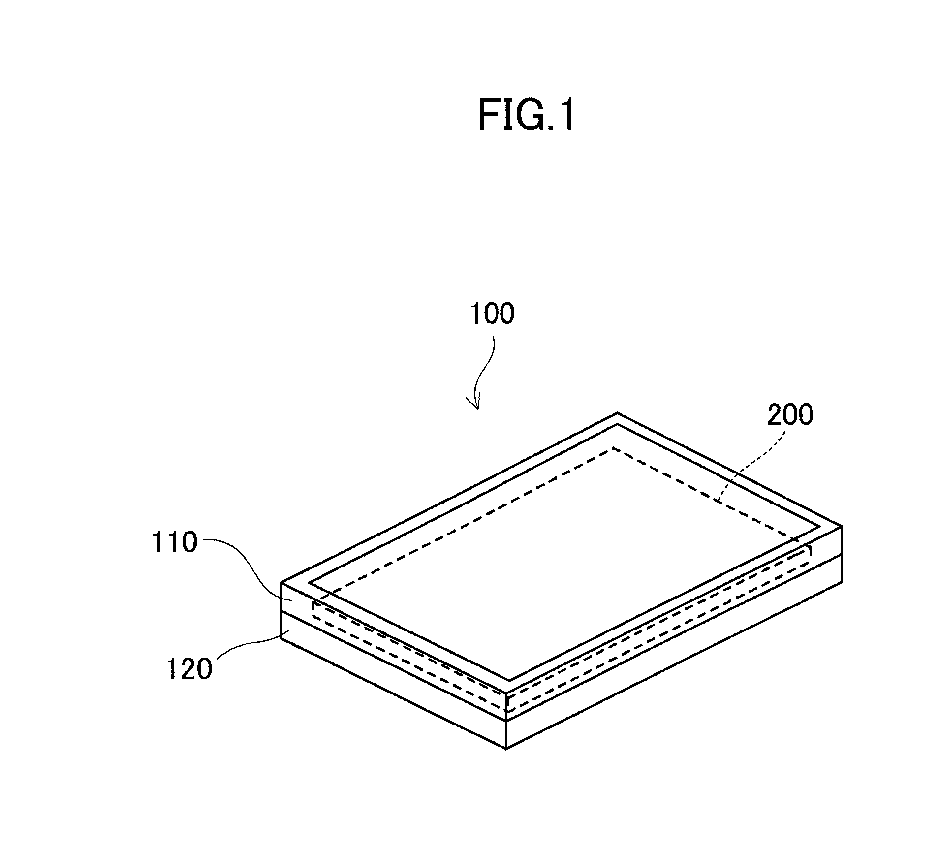
[0029]FIG. 1 schematically illustrates an organic EL display device 100 according to an embodiment of the present invention. As illustrated in FIG. 1, the organic EL display device 100 includes an organic EL panel 200 fixed between an upper frame 110 and a lower frame 120.

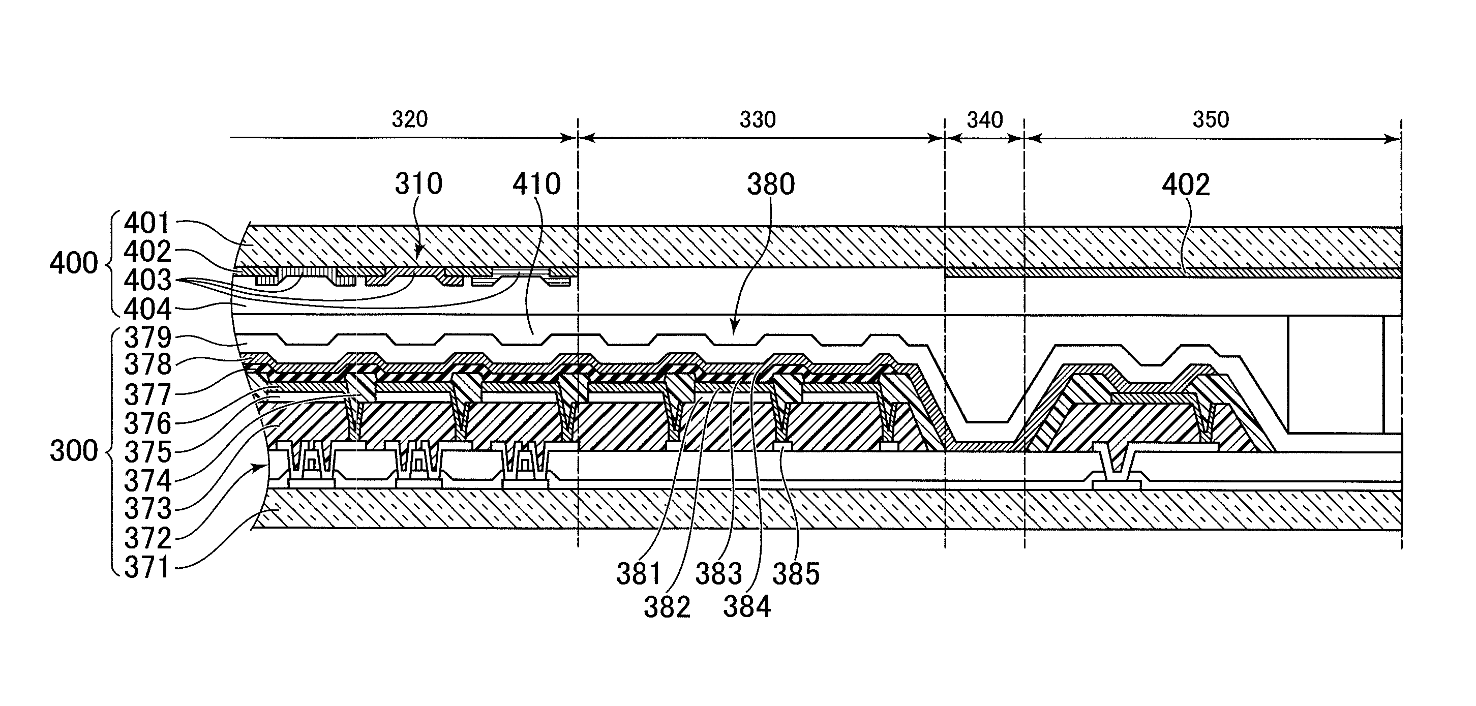
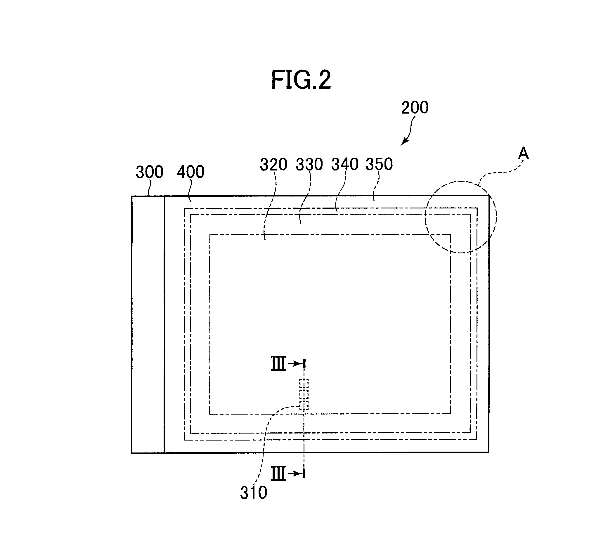
[0030]FIG. 2 is a plan view illustrating a configuration of the organic EL panel 200. The organic EL panel 200 includes a TFT substrate 300, and a sealing substrate 400 adhered to the TFT substrate 300 with a transparent resin 410 (to be described later). As illustrated in FIG. 2, the organic EL panel 200 includes a display area 320 in which pixels 310 each having an anode electrode 376 (to be described later) arranged therein, and emitting light on the b...


PUM

PropertyMeasurementUnit
areaaaaaaaaaaa
sizeaaaaaaaaaa
response speedaaaaaaaaaa

Abstract

A display device includes a display area in which pixels are arranged in a matrix, and an inspection area that is formed around the display area, and has an inspection pixel, in which the display area includes plural first electrodes that are disposed in the respective pixels, a light emitting organic layer that includes plural organic material layers having a light emitting layer, and a second electrode that covers the display area, and the inspection pixel includes an inspection first electrode electrically independent from the respective first electrodes, an inspection organic layer in which at least one light emitting layer of the plural organic material layers is continuous from the display area, and comes in contact with the inspection first electrode, and an inspection second electrode that is continuous from the second electrode, and comes in contact with the inspection organic layer.

Description

BACKGROUND OF THE INVENTION[0001]1. Field of the Invention[0002]The present invention relates to a display device.[0003]2. Description of the Related Art[0004]In recent years, an image display device (hereinafter referred to as “organic EL (electro-luminescent) display device”) using self-emitting bodies called “organic light emitting diodes (OLED)” has been put into a practical use. As compared with a liquid crystal display device in a related art, the organic EL display device uses the self-emitting bodies, and therefore not only is excellent in visibility and response speed, but also does not require an auxiliary lighting device such as backlight. As a result, the organic EL display device can be further thinned.[0005]Because an organic EL element used in the organic EL display device of this type is deteriorated when absorbing moisture, measures are taken to hermetically bond a sealing glass substrate onto a TFT (thin film transistor) substrate on which a light emitting layer is...

Claims


Application Information

Patent Timeline
Patent Type & Authority Patents(United States)
IPC IPC(8): H01L27/32H01L27/28G02F1/13G02F1/1341
CPCH01L27/3223H01L27/3244H01L2251/562H10K59/88H10K59/12H10K71/831
Inventor FURUIE, MASAMITSU
Owner JAPAN DISPLAY INC
Learn More