Semiconductor device and method for manufacturing the same

a semiconductor device and semiconductor technology, applied in the direction of semiconductor devices, electrical equipment, transistors, etc., can solve the problems of contact resistance, performance degradation of semiconductor devices, so as to suppress the occurrence of leakage current and eliminate the pathway for leakage current

Active Publication Date: 2016-04-05
INST OF MICROELECTRONICS CHINESE ACAD OF SCI
View PDF14 Cites 0 Cited by
  • Summary
  • Abstract
  • Description
  • Claims
  • Application Information

AI Technical Summary

Benefits of technology

[0006]The present invention is intended to provide a semiconductor device and a method for manufacturing the same, which are capable of eliminating pathway for leakage current between SOI substrate and source / drain regions at the meantime of reducing contact resistance at source / drain regions.
[0013]As compared to the prior art, the present invention exhibits following advantages:
[0014]1) Bottoms of source / drain regions are located within the insulating layer of the SOI substrate, and a crystal dielectric layer is formed between source / drain regions and the SOI substrate, such that bottoms of the source / drain regions are separated from the SOI substrate, which therefore effectively eliminates pathway for leakage current between source / drain regions and the SOI substrate, and suppresses occurrence of leakage current accordingly;2) source / drain regions are formed in the active layer and a part of the insulating layer of the SOI substrate, which accordingly eliminating the defect in the prior art of forming fairly thin source / drain regions merely in active layer, therefore reduces contact resistance at source / drain regions and enhances performance of semiconductor devices accordingly.

Problems solved by technology

However, since leakage current that occurs between source / drain regions 110 and the bulk Si substrate 100 may deteriorate performance of semiconductor devices, bulk Si substrates have been replaced by Silicon-On-Insulator (SOI) in the prior art for reducing leakage current between substrates and source / drain regions.
Consequently, contact resistance at the source / drain regions 110 may increase, and performance of semiconductor devices may deteriorate.

Method used


Image

  • Semiconductor device and method for manufacturing the same
  • Semiconductor device and method for manufacturing the same
  • Semiconductor device and method for manufacturing the same

Examples


Embodiment Construction

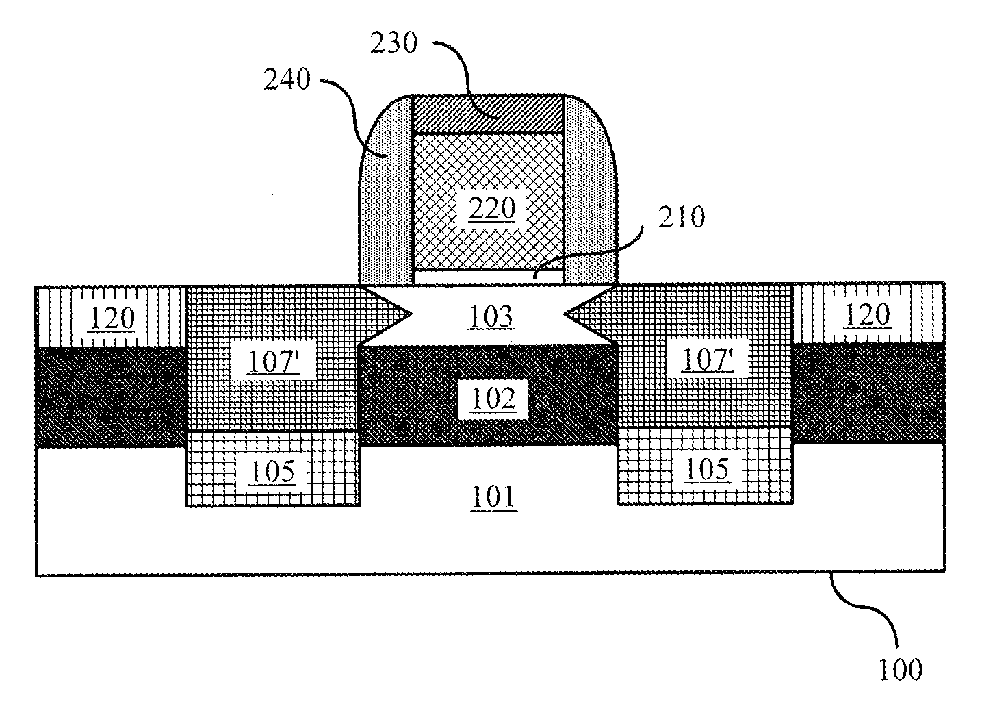
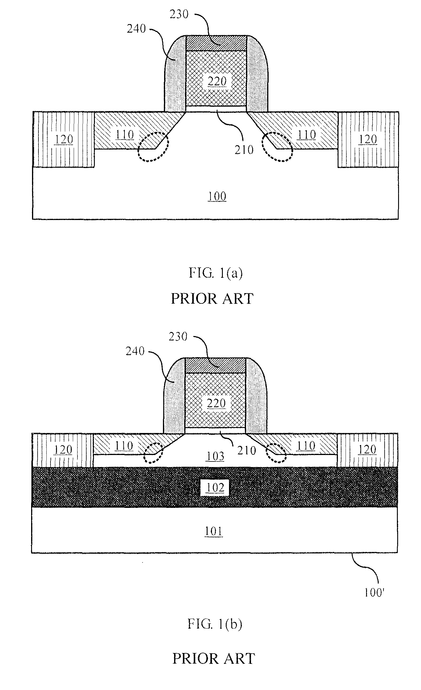
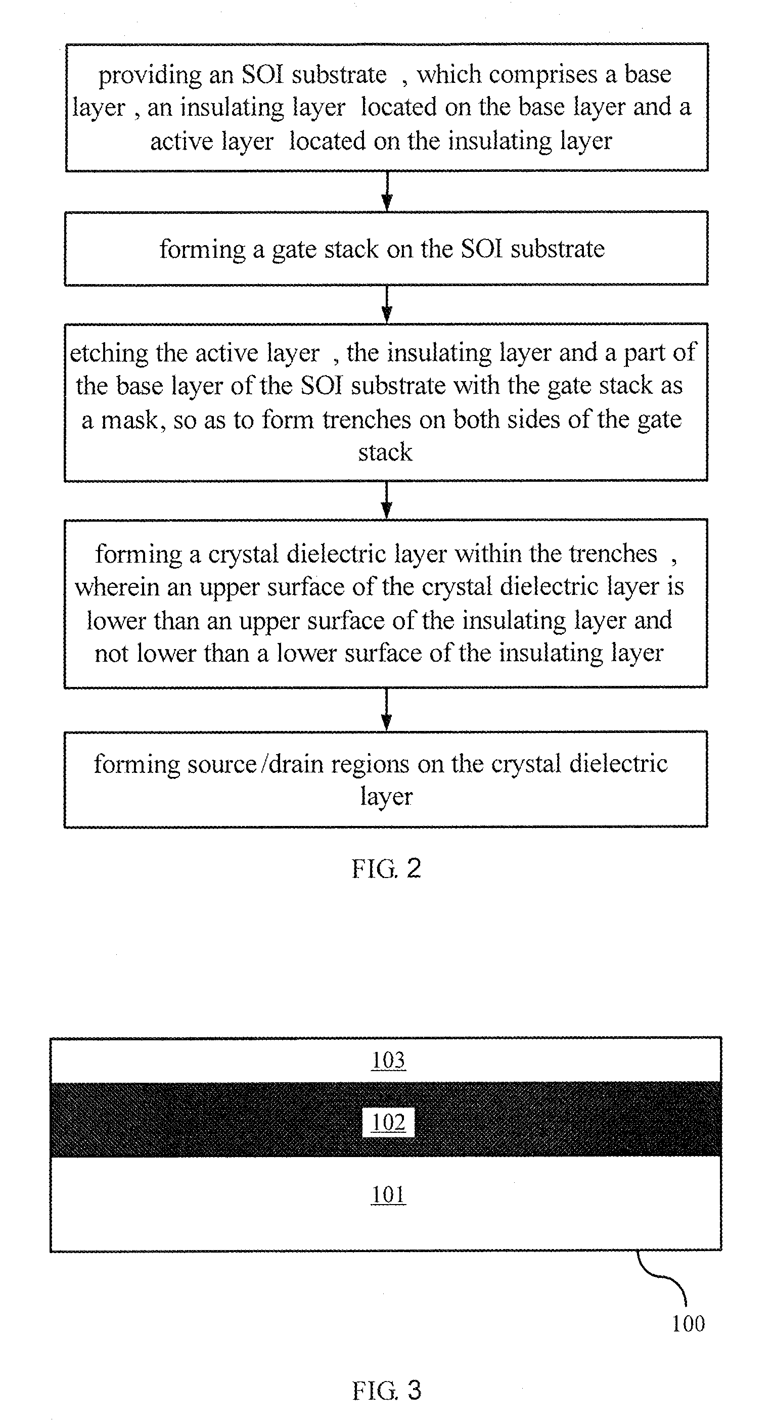
[0020]Embodiments of the present invention will be described in detail below. Examples of embodiments are illustrated in the drawings, and the same or similar reference numbers throughout denote the same or similar elements or elements having the same or similar functions. It should be noted that embodiments described below in conjunction with the drawings are illustrative, and are provided for explaining the present invention only, and thus shall not be interpreted as a limit to the present invention.

[0021]Various embodiments or examples are provided here below to implement different structures of the present invention. To simplify the disclosure of the present invention, descriptions of components and arrangements of specific examples are given below. Of course, they are only illustrative and are not intended to limit the present invention. Moreover, in the present invention, reference numbers and / or letters may be repeated in different examples. Such repetition is for purposes of...


PUM


Abstract

The present invention provides a method for manufacturing a semiconductor device, which comprises: providing an SOI substrate, which comprises a base layer, an insulating layer located on the base layer and a active layer located on the insulating layer; forming a gate stack on the SOI substrate; etching the active layer, the insulating layer and a part of the base layer of the SOI substrate with the gate stack as a mask, so as to form trenches on both sides of the gate stack; forming a crystal dielectric layer within the trenches, wherein the upper surface of the crystal dielectric layer is lower than the upper surface of the insulating layer and not lower than the lower surface of the insulating layer; and forming source / drain regions on the crystal dielectric layer. The present invention further provides a semiconductor device. The present invention is capable of eliminating pathway for leakage current between source / drain regions and SOI substrate at the meantime of reducing contact resistance at source / drain regions.

Description

CROSS REFERENCE TO RELATED APPLICATION[0001]This application is a national stage application, filed under 35 U.S.C. §371, of PCT Patent Application Serial No. PCT / CN2012 / 081506, filed on Sep. 17, 2012, entitled “SEMICONDUCTOR DEVICE AND METHOD FOR MANUFACTURING THE SAME”, which claimed priority to Chinese Patent Application Serial No. 201210304241.6, filed on Aug. 23, 2012, all of which are hereby incorporated by reference in their entirety.FIELD OF THE INVENTION[0002]The present invention relates to semiconductor manufacturing field, particularly, to a semiconductor device and a method for manufacturing the same.BACKGROUND OF THE INVENTION[0003]In traditional semiconductor manufacturing field, forming strained source / drain regions in semiconductor devices has become a significant mean for improving performance of semiconductor devices by generating compressive stress or tensile stress onto channels, which accordingly enhances carriers mobility inside channels. Specific processes fo...

Claims


Application Information

Patent Timeline
Patent Type & Authority Patents(United States)
IPC IPC(8): H01L21/00H01L29/161H01L29/78H01L29/16H01L29/08H01L29/06H01L21/762H01L21/311H01L21/306H01L21/02H01L29/786H01L29/66H01L29/165H01L29/00H01L29/417
CPCH01L29/41783H01L21/02181H01L21/02192H01L21/02194H01L21/30604H01L21/31111H01L21/31116H01L21/76224H01L29/0653H01L29/0847H01L29/16H01L29/161H01L29/165H01L29/6656H01L29/66636H01L29/66772H01L29/66825H01L29/7848H01L29/78654H01L29/66553H01L29/78
Inventor ZHONG, HUICAIZHAO, CHAOLIANG, QINGQING
Owner INST OF MICROELECTRONICS CHINESE ACAD OF SCI
Why Eureka
Try Eureka