Magnetic field controlled reconfigurable semiconductor logic device and method for controlling the same

a semiconductor logic and magnetic field technology, applied in logic circuits, logic circuits using saturable magnetic devices, logic circuit coupling/interface arrangements, etc., can solve problems such as difficulty in achieving high performance of computers

Active Publication Date: 2016-05-03
UNITED STATES OF AMERICA +1
View PDF24 Cites 4 Cited by
  • Summary
  • Abstract
  • Description
  • Claims
  • Application Information

AI Technical Summary

Benefits of technology

[0008]The present invention has been made in an effort to provide a magnetic field controlled nonvolatile reconfigurable semiconductor logic device having advantages of executing logical operations and a memory function. An exemplary embodiment of the present invention provides a method for controlling the reconfigurable semiconductor logic device.

Problems solved by technology

Accordingly, bottlenecks occur during signal transmission between an operation circuit and a memory circuit, and thus it is difficult to achieve high performance of the computer even if performances of the logic devices and memory devices are improved.

Method used


Image

  • Magnetic field controlled reconfigurable semiconductor logic device and method for controlling the same
  • Magnetic field controlled reconfigurable semiconductor logic device and method for controlling the same
  • Magnetic field controlled reconfigurable semiconductor logic device and method for controlling the same

Examples


experimental example

Experiment on Logic Device for AND Operation

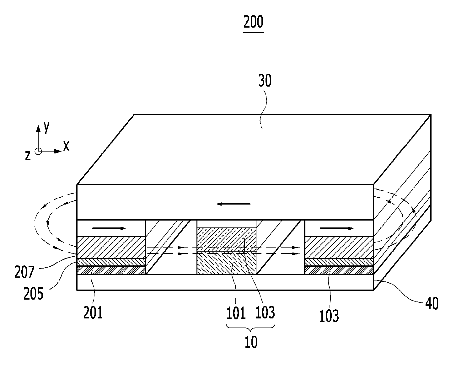
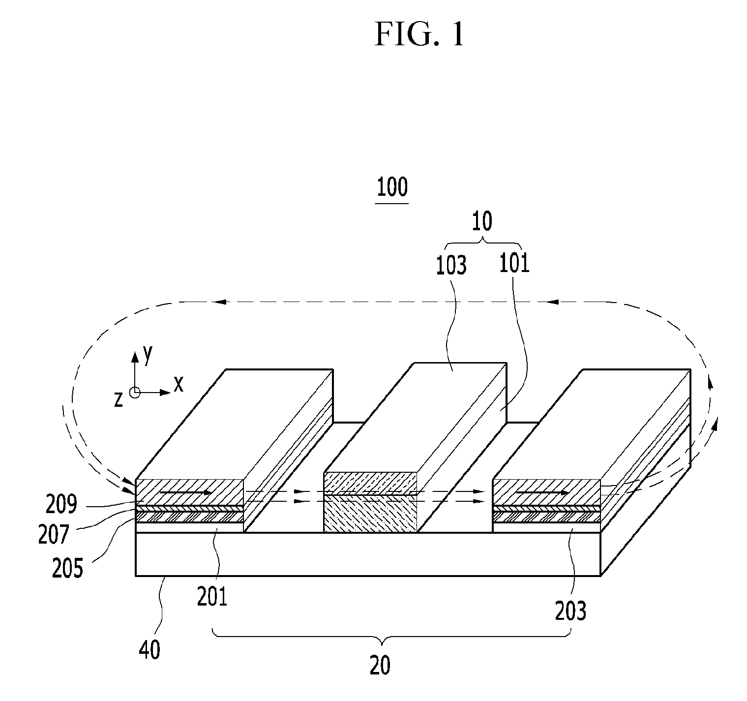
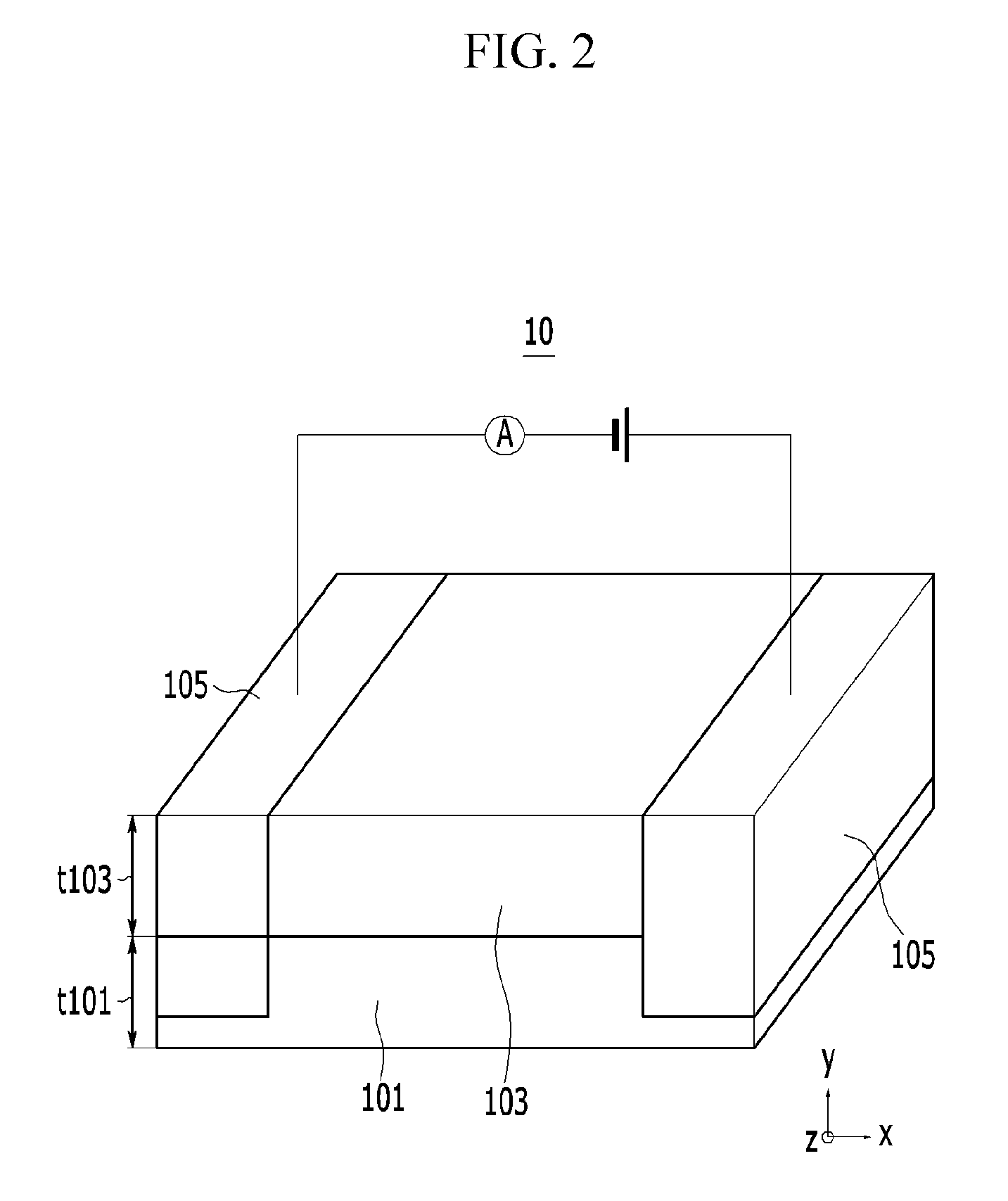
[0093]A reconfigurable semiconductor logic device having the same structure as the reconfigurable semiconductor logic device of FIG. 5 was manufactured. Here, a semiconductor device having a channel width of 10 μm and a length of 120 μm was manufactured using photolithography. Meanwhile, the semiconductor device was manufactured by laminating an n-type InSb layer having a thickness of 0.2 μm on a p-type InSb layer having a thickness of 6 μm. A method for manufacturing a magnetic field controlled device can be easily understood by those skilled in the art, and thus a detailed description thereof is omitted.

[0094]The threshold voltages of the semiconductor devices NP1 and NP2 were 11.0 V when a positive direction magnetic field was applied thereto, and 11.3 V when a negative direction magnetic field was applied thereto. The positive or negative direction magnetic field was applied to the semiconductor devices NP1 and NP2 while applying a vol...


PUM


Abstract

A non-volatile reconfigurable logic device executing logical operations and a memory function and controlled by a magnetic field is provided. The reconfigurable logic device includes i) at least one semiconductor device; and ii) a pair of magnetic field controlled devices respectively spaced apart from both sides of the semiconductor device and that are adapted to generate magnetic field leakage to control the semiconductor device. The semiconductor device includes i) a first semiconductor layer; and ii) a second semiconductor layer located on the first semiconductor layer. One of the first semiconductor layer and the second semiconductor layer is a p-type semiconductor layer and the other is an n-type semiconductor layer.

Description

CROSS-REFERENCE TO RELATED APPLICATION[0001]This application claims priority to and the benefit of Korean Patent Application No. 10-2012-0147963 filed in the Korean Intellectual Property Office on Dec. 18, 2012, the entire contents of which are incorporated herein by reference.BACKGROUND OF THE INVENTION[0002](a) Field of the Invention[0003]The present invention relates to a magnetic field controlled reconfigurable semiconductor logic device. More specifically, the present invention relates to a magnetic field controlled nonvolatile reconfigurable semiconductor logic device which executes logical operations and a memory function.[0004](b) Description of the Related Art[0005]Recently, a variety of potable information devices such as tablet PC (personal computer), smartphones, etc. have been developed. Development of these portable information devices is based on miniaturization and high performance of logic devices (transistors) and memories which are basic elements of a computer cir...

Claims


Application Information

Patent Timeline
Patent Type & Authority Patents(United States)
IPC IPC(8): H03K19/173H01L43/02H01L27/22H03K19/0175H03K19/16H01L43/08G11C11/16
CPCH01L43/02G11C11/161H01L27/22H01L43/08H03K19/017581H03K19/16G11C11/1695H10B61/00H10N59/00H10N50/80H10N50/10G11C11/15H10N50/01
Inventor CHANG, JOON YEONHONG, JIN KISONG, JIN DONGJOHNSON, MARK
Owner UNITED STATES OF AMERICA
Why Eureka
Try Eureka