Emitting device with improved extraction

a technology of light extraction and emitting device, which is applied in the direction of cad circuit design, lighting and heating apparatus, instruments, etc., can solve the problems of affecting the propagation of radiation, affecting the optical properties of materials, and affecting the effect of radiation propagation

Active Publication Date: 2016-05-10
SENSOR ELECTRONICS TECH
View PDF48 Cites 21 Cited by
  • Summary
  • Abstract
  • Description
  • Claims
  • Application Information

AI Technical Summary

Problems solved by technology

Changes in molar fractions of semiconductor alloys can allow for band gap control, but can lead to abrupt changes in the optical properties of the materials and result in light trapping.
A small TIR angle results in a large fraction of light rays reflecting from the interface boundaries, thereby leading to light trapping and subsequent absorption by layers or LED metal contacts.
Nevertheless, light only can be partially transmitted through the interface, even if it does not undergo TIR, due to Fresnel losses.

Method used


Image

  • Emitting device with improved extraction
  • Emitting device with improved extraction
  • Emitting device with improved extraction

Examples


Embodiment Construction

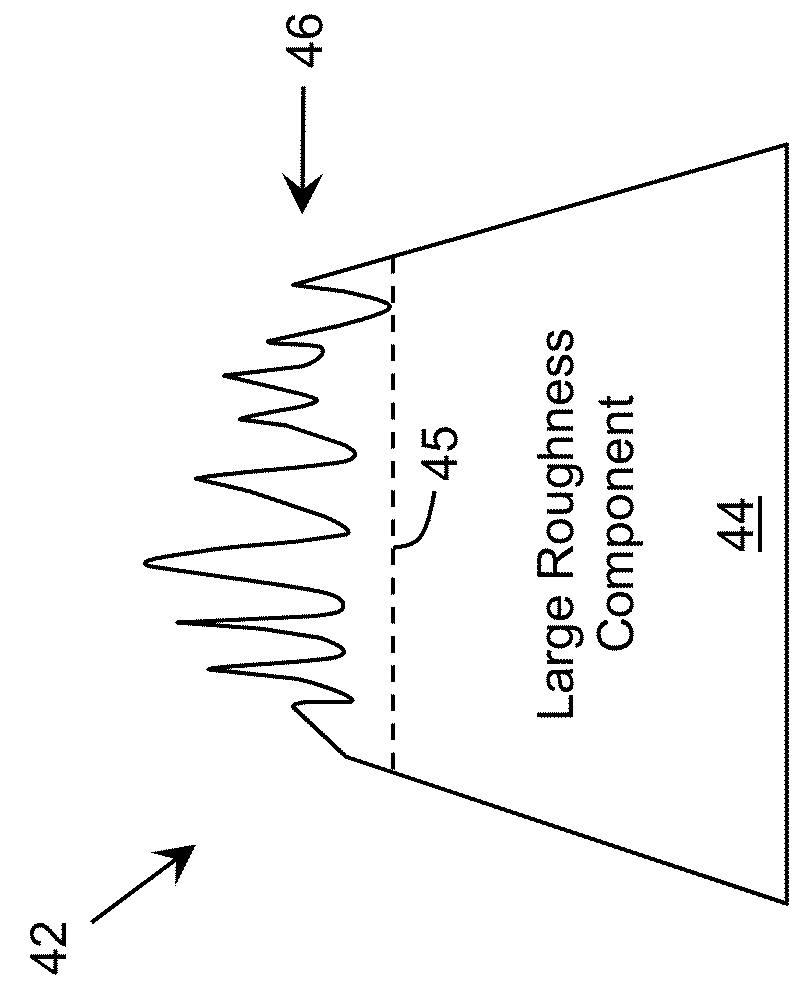
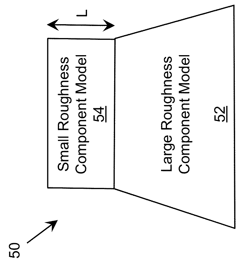
[0025]As indicated above, aspects of the invention provide a profiled surface for improving the propagation of radiation through an interface. The profiled surface includes a set of large roughness components providing a first variation of the profiled surface having a characteristic scale approximately an order of magnitude larger than a target wavelength of the radiation. The set of large roughness components can include a series of truncated shapes. The profiled surface also includes a set of small roughness components superimposed on the set of large roughness components and providing a second variation of the profiled surface having a characteristic scale on the order of the target wavelength of the radiation. As used herein, unless otherwise noted, the term “set” means one or more (i.e., at least one) and the phrase “any solution” means any now known or later developed solution.

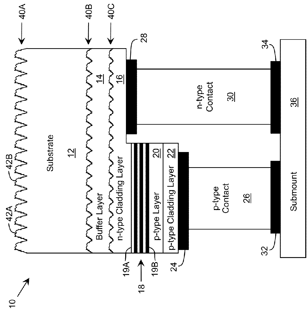
[0026]Turning to the drawings, FIG. 1 shows a schematic structure of an illustrative emitting device...


PUM

PropertyMeasurementUnit
radiation wavelengthsaaaaaaaaaa
transparentaaaaaaaaaa

Abstract

A profiled surface for improving the propagation of radiation through an interface is provided. The profiled surface includes a set of large roughness components providing a first variation of the profiled surface having a characteristic scale approximately an order of magnitude larger than a target wavelength of the radiation. The set of large roughness components can include a series of truncated shapes. The profiled surface also includes a set of small roughness components superimposed on the set of large roughness components and providing a second variation of the profiled surface having a characteristic scale on the order of the target wavelength of the radiation.

Description

REFERENCE TO RELATED APPLICATIONS[0001]The current application is a continuation-in-part of co-pending U.S. application Ser. No. 13 / 517,711, titled “Emitting Device with Improved Extraction,” which was filed on 14 Jun. 2012, and which claims the benefit of co-pending U.S. Provisional Application No. 61 / 497,489, titled “Light Emitting Diodes with Improved Extraction,” which was filed on 15 Jun. 2011, both of which are hereby incorporated by reference.GOVERNMENT LICENSE RIGHTS[0002]This invention was made with Federal government support under Contract No. W911 NF-10-2-0023 awarded by Defense Advanced Research Projects Agency (DARPA). The government has certain rights in the invention.TECHNICAL FIELD[0003]The disclosure relates generally to emitting devices, and more particularly, to an emitting device with improved light extraction.BACKGROUND ART[0004]Semiconductor emitting devices, such as light emitting diodes (LEDs) and laser diodes (LDs), include solid state emitting devices compo...

Claims


Application Information

Patent Timeline
Patent Type & Authority Patents(United States)
IPC IPC(8): H01L33/62H01L33/22G06F17/50F21V5/00H01L33/00H01L33/20H01L33/10
CPCH01L33/22F21V5/002G06F17/5009G06F17/5045H01L33/007H01L33/10H01L33/20H01L2933/0083Y10T29/49G06F30/20G06F30/30H01L2933/0058
Inventor SHATALOV, MAXIM S.DOBRINSKY, ALEXANDERSHUR, MICHAELGASKA, REMIGIJUS
Owner SENSOR ELECTRONICS TECH
Why Eureka
Try Eureka