Light-emitting element, comprising an organometallic complex light-emitting material, a light-emitting device and an electronic device comprising the light-emitting element

a light-emitting element and organometallic complex technology, applied in the field of light-emitting elements, can solve the problems of insufficient stability of bcp, inability to obtain light-emitting with high efficiency, and insufficient lifetime of elements, so as to reduce driving voltage, improve light-emitting efficiency, and long life

Active Publication Date: 2016-05-31
SEMICON ENERGY LAB CO LTD
View PDF77 Cites 121 Cited by
  • Summary
  • Abstract
  • Description
  • Claims
  • Application Information

AI Technical Summary

Benefits of technology

[0015]Further, when considering that electronic devices to which such light-emitting elements are applied are practically used, power consumption thereof may be an important element. Therefore, as a factor affecting power consumption, not only light emission efficiency but also reduced driving voltage of the element becomes very important.
[0047]Furthermore, an electronic device which is an embodiment of the present invention is a light-emitting device with low power consumption and a long lifetime.

Problems solved by technology

According to the report in Non Patent Document 1 described above, the half-life period of luminance is about 170 hours when the initial luminance is set to be 500 cd / m2 in constant current driving, and so, there is a problem of the lifetime of the element.
In addition, Non Patent Document 1 reports a problem of lifetime, in which bathocuproine (abbreviation: BCP) is used as a hole-blocking layer, because the stability of BCP is not sufficient.
However, if BCP is removed from an element structure in Non Patent Document 1, light emission with high efficiency cannot be obtained.
Thus, with the element structure of Non Patent Document 1, although high efficiency can be achieved due to BCP, a light-emitting element having a long lifetime cannot be obtained because of BCP.
However, the performance of a phosphorescent compound cannot be utilized efficiently.
For the above reasons, it can be seen that it is very difficult to achieve both high light emission efficiency and a long lifetime.

Method used


Image

  • Light-emitting element, comprising an organometallic complex light-emitting material, a light-emitting device and an electronic device comprising the light-emitting element
  • Light-emitting element, comprising an organometallic complex light-emitting material, a light-emitting device and an electronic device comprising the light-emitting element
  • Light-emitting element, comprising an organometallic complex light-emitting material, a light-emitting device and an electronic device comprising the light-emitting element

Examples


embodiment 1

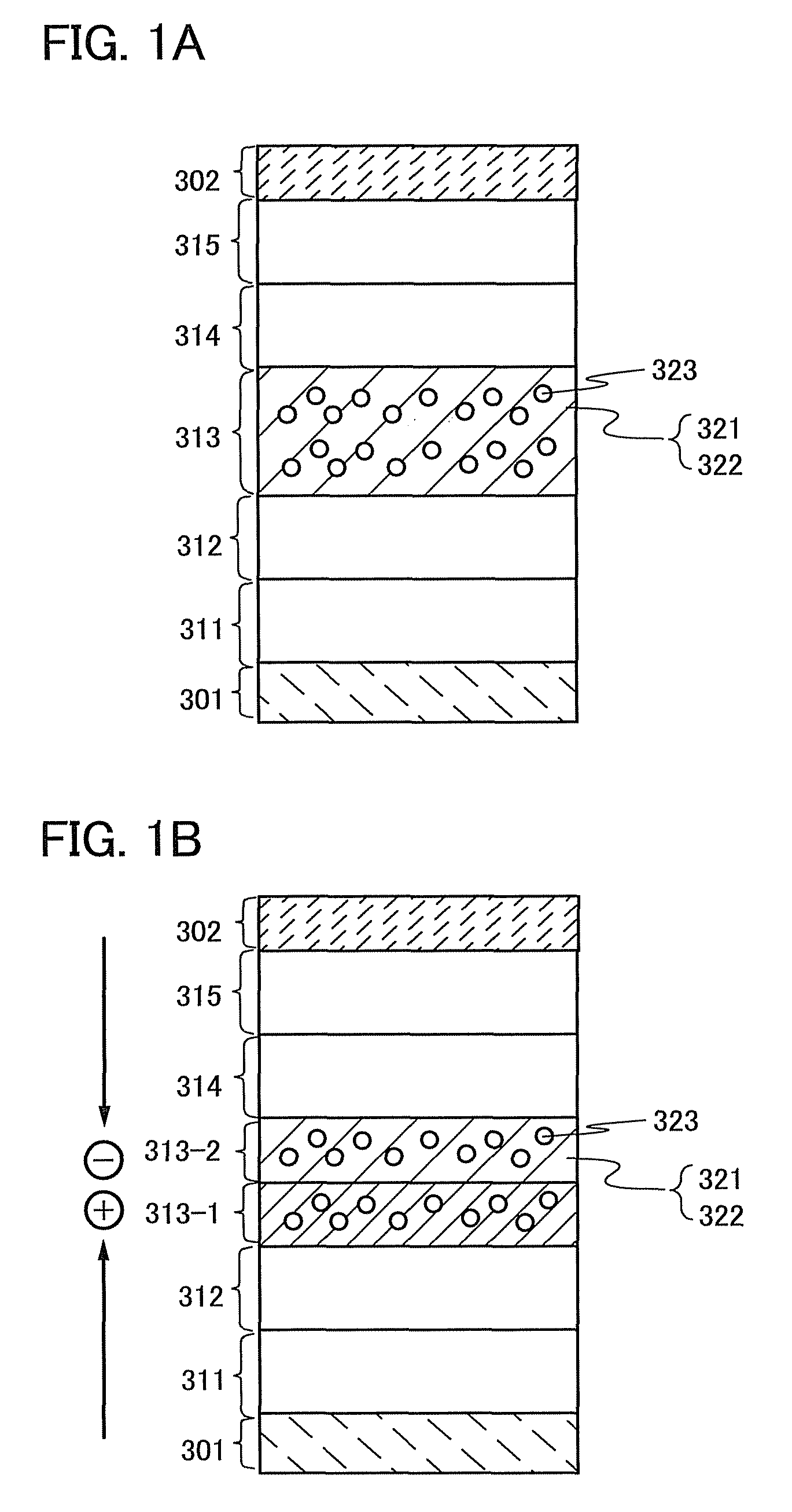
[0092]In a light-emitting element in which a layer containing an organic compound is provided between a pair of electrodes, a structure in which the layer containing the organic compound is formed with a plurality of layers in which functions are separated has been mainstream. As the layers in which functions are separated, there are various kinds, for example, a carrier-injection layer and a carrier-transporting layer in addition to a light-emitting layer having a light-emitting function. The layer containing the organic compound does not have to include all these layers, or may include layers other than these layers.

[0093]In a light-emitting element including such layers in which functions are separated, characteristics of these layers are different from each other; thus, carriers are accumulated at an interface between the layers (in particular, at an interface between a light-emitting layer and the other layers) in some cases. Accordingly, the lifetime of the light-emitting elem...

embodiment 2

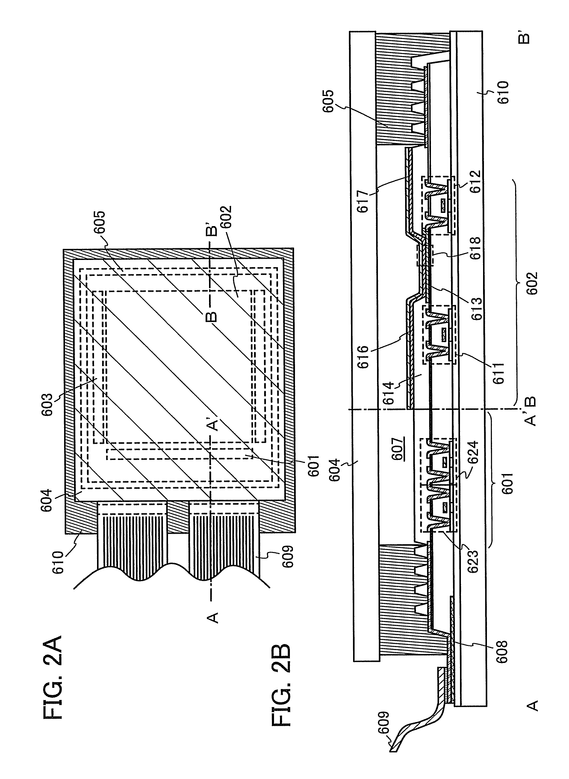
[0131]In this embodiment, an image display device is described as an example of a light-emitting device having the light-emitting element described in Embodiment 1.

[0132]In this embodiment, an image display device having a light-emitting element in a pixel portion is described with reference to FIGS. 2A and 2B. Note that FIG. 2A is a top view illustrating an image display device while FIG. 2B is a cross-sectional view taken along lines A-A′ and B-B′ in FIG. 2A. This image display device includes: a pixel portion 602 shown with a dotted line; and a driver circuit portion (source side driver circuit) 601 shown with a dotted line and a driver circuit portion (gate side driver circuit) 603 shown with a dotted line for controlling light emission of the light-emitting element. Further, reference numeral 604 denotes a sealing substrate; 605, a sealing material; and 607, a space surrounded by the sealing material 605.

[0133]Note that a leading wiring 608 is a wiring for transmitting signals ...

embodiment 3

[0146]The light-emitting element described in Embodiment 1 has high light emission efficiency, a long lifetime, and low driving voltage; therefore, the light-emitting element is suitable for a lighting device which is an example of a light-emitting device. Accordingly, in this embodiment, an application example of a lighting device using the light-emitting element described in Embodiment 1 is described.

[0147]FIG. 4A shows an example of a liquid crystal display device in which the light-emitting element described in Embodiment 1 is used as a backlight which is one kind of lighting devices. The liquid crystal display device illustrated in FIG. 4A includes a housing 401, a liquid crystal layer 402, a backlight 403, and a housing 404, in which the liquid crystal layer 402 is connected to a driver IC 405. The light-emitting element described in Embodiment 1 is used as the backlight 403. Current is supplied to the backlight 403 through a terminal 406.

[0148]By using the light-emitting elem...


PUM


Abstract

To provide a light-emitting element with high light emission efficiency, a long lifetime, and reduced driving voltage. To provide a light-emitting element including an anode, a cathode, and a plurality of light-emitting layers which are in contact with each other so that a stacked structure is formed, between the anode and the cathode, in which the plurality of light-emitting layers are formed with a first light-emitting layer which is close to the anode and a second light-emitting layer which is close to the cathode, the first light-emitting layer and the second light-emitting layer each include a host material, a hole-transporting material, and a light-emitting material, and the concentration of the hole-transporting material in the first light-emitting layer is higher than the concentration of the hole-transporting material in the second light-emitting layer.

Description

TECHNICAL FIELD[0001]The present invention relates to a light-emitting element which includes a layer containing an organic compound between a pair of electrodes. Further, the present invention relates to a light-emitting device using the light-emitting element. Furthermore, the present invention relates to an electronic device using the light-emitting device.BACKGROUND ART[0002]In recent years, a light-emitting element using a light-emitting organic compound or inorganic compound as a light-emitting material has been actively developed. In particular, a light-emitting element called an EL element has a simple structure in which a light-emitting layer containing a light-emitting material is provided between electrodes. Therefore, the light-emitting element has attracted attention as a next-generation flat panel display element because of its characteristics such as a thin shape, lightweight, high response speed, and direct current driving at low voltage. In addition, a display using...

Claims


Application Information

Patent Timeline
Patent Type & Authority Patents(United States)
IPC IPC(8): H01L51/54H01L51/50H01L51/00
CPCH01L51/5012H01L51/5016H01L51/0081H01L51/0085H01L51/5036H01L2251/552H10K85/324H10K85/342H10K50/11H10K50/125H10K2101/10H10K2101/30C09K11/06H10K50/12
Inventor OHSAWA, NOBUHARUINOUE, HIDEKOSEO, SATOSHI
Owner SEMICON ENERGY LAB CO LTD
Why Eureka
Try Eureka