Eureka AIR delivers breakthrough ideas for toughest innovation challenges, trusted by R&D personnel around the world.

Address arithmetic on block RAMs

Active Publication Date: 2016-06-14
TAHOE RES LTD
View PDF9 Cites 4 Cited by
  • Summary
  • Abstract
  • Description
  • Claims
  • Application Information

AI Technical Summary

Benefits of technology

The patent text explains methods and systems for reducing the need for multiple address lines to be routed to embedded memory blocks. This can help to improve performance and efficiency, reduce power consumption, and avoid routing congestion.

Problems solved by technology

Routing address lines consumes general interconnect resources, which are limited, and the toggling of the address lines in the general interconnect adds to overall power consumption.
Additionally, routing address lines often results in routing congestion causing critical timing delays in the design being implemented within an FPGA.

Method used


Image

  • Address arithmetic on block RAMs
  • Address arithmetic on block RAMs
  • Address arithmetic on block RAMs

Examples


Embodiment Construction

[0028]To provide an overall understanding of the invention, certain illustrative embodiments will now be described. However, it will be understood by one of ordinary skill in the art that the systems and methods described herein may be adapted and modified as is appropriate for the application being addressed and that the systems and methods described herein may be employed in other suitable applications, and that such other additions and modifications will not depart from the scope hereof.

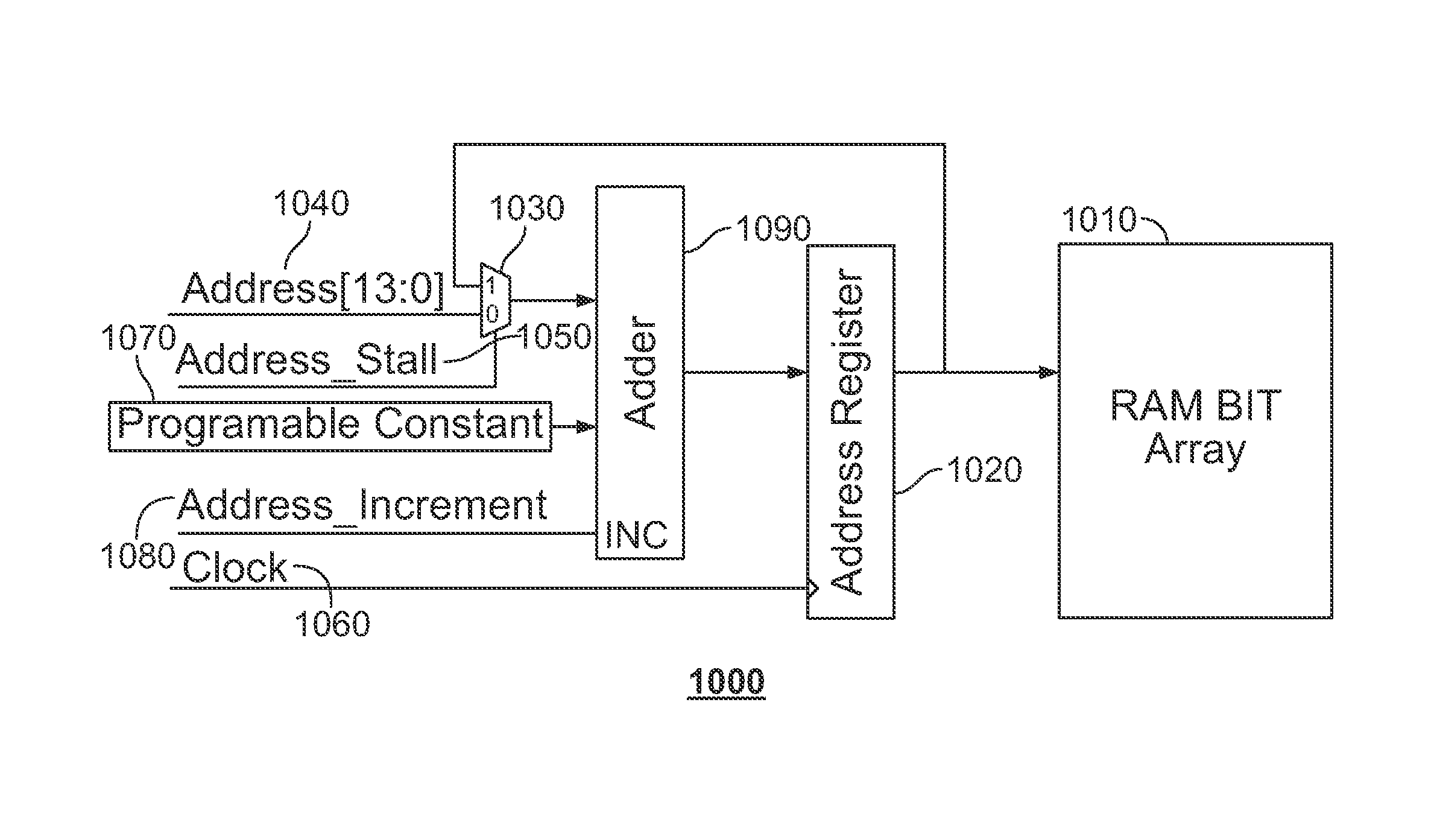
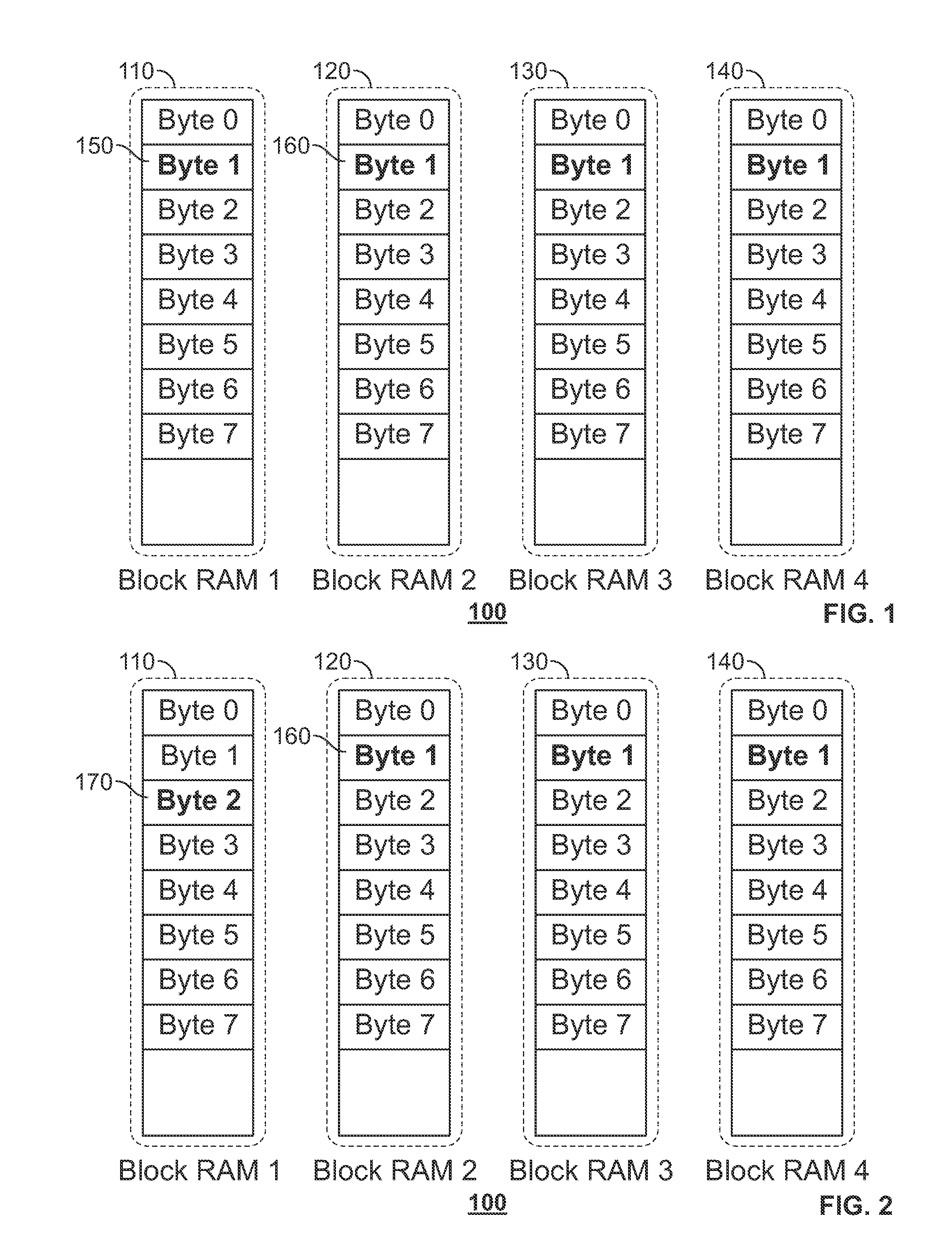
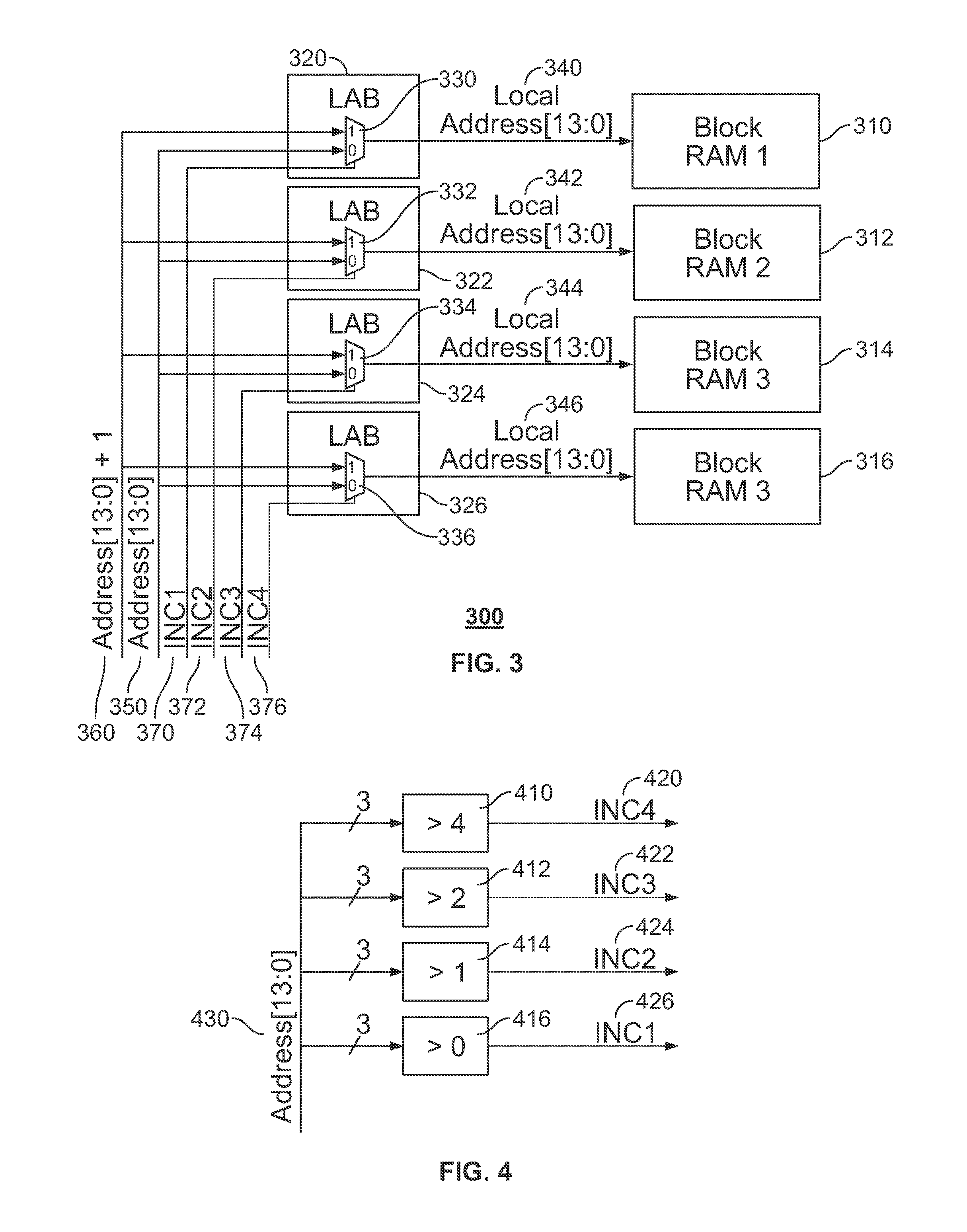
[0029]FIG. 1 is a simplified block diagram of wide memory, according to an illustrative embodiment. Wide memory 100 includes block RAMs 110, 120, 130, and 140. Each block RAM may contain, for example, 16K bits addressable in various address depth and word width configurations. For example, each block RAM 110, 120, 130, and 140 may contain 8 address locations having 2K bits each.

[0030]Each block RAM in wide memory 100 may contain several addresses. For example, the hexadecimal address 0x0000 may co...


PUM


Abstract

Systems and methods are disclosed for reducing or eliminating address lines that need to be routed to multiple related embedded memory blocks. In particular, one or more inputs are added to a block Random Access Memory (RAM) such that when one or more of the inputs are asserted, the address input to the Block RAM may be incremented prior to being used to retrieve data contents of the block RAM. Thus, if address <addr> is provided to the block RAM and the address increment signal is asserted, data may be read from location <addr+N> instead of <addr>, where N may be an integer. Block RAMs with such address arithmetic may be used to implement wide First-In-First-Out (FIFO) queues, wide memories, and / or data-burst accessible block RAMs.

Description

BACKGROUND OF THE DISCLOSURE[0001]A Field Programmable Gate Array (FPGA) or logic device is an integrated circuit consisting of programmable logic blocks and programmable routing. Programmable logic blocks may include blocks of logic elements, for performing programmable logic operations, and block Random Access Memories (RAMs) for storing and retrieving data. In an illustrative example, block RAMs may contain 16,000 (16K) bits addressable in various address depth and word width configurations. For example, a 16K block RAM may be addressable in a 8x2K configuration, i.e., 8 address locations of 2,000 bits each, or a 1x16K configuration, i.e., 1 address location of 16,000 bits.[0002]Block RAMs may receive inputs from address ports and data ports. Each block RAM may have two address ports and two data ports—one address port and one data port for reading and one address port and one data port for writing.[0003]If wide data ports, i.e., data ports capable of processing a large number of...

Claims


Application Information

Patent Timeline
IPC IPC(8): G06F12/06G11C7/10
CPCG06F12/06G11C7/1036G11C8/04G11C8/06G11C8/18G11C7/10G11C7/1072
Inventor PEDERSEN, BRUCE B.
Owner TAHOE RES LTD
Why Eureka
Eureka Blog
Learn More