Semiconductor device with voids within silicon-on-insulator (SOI) structure and method of forming the semiconductor device

a technology of silicon-on-insulator and semiconductor device, which is applied in the direction of semiconductor device, basic electric element, electrical apparatus, etc., can solve the problems of increasing manufacturing cost by at least 10% or more, adding expensive equipment, and reducing the production cost, so as to improve the fom, reduce parasitic capacitance, and reduce the effect of capacitan

Active Publication Date: 2016-06-14
KEY FOUNDRY CO LTD
View PDF6 Cites 1 Cited by
  • Summary
  • Abstract
  • Description
  • Claims
  • Application Information

AI Technical Summary

Benefits of technology

[0010]An object of the present disclosure is to reduce Parasitic Capacitance under the active area on the SOI semiconductor and by improving the FOM.
[0011]Another object of the present disclosure is to reduce capacitance in an off state that is a main parameter for a performance index with respect to a switch device.

Problems solved by technology

However, the implementation of such improvements would require additional expensive equipment, which would increase the cost of manufacturing.
Furthermore, if a Trap-Rich layer is added into the SOI semiconductor (typically as an additional layer at the interface of the BOX layer and of the Handle Silicon substrate layer) in order to enhance an RF characteristic, the cost increases by at least 10% or more.

Method used


Image

  • Semiconductor device with voids within silicon-on-insulator (SOI) structure and method of forming the semiconductor device
  • Semiconductor device with voids within silicon-on-insulator (SOI) structure and method of forming the semiconductor device
  • Semiconductor device with voids within silicon-on-insulator (SOI) structure and method of forming the semiconductor device

Examples


Embodiment Construction

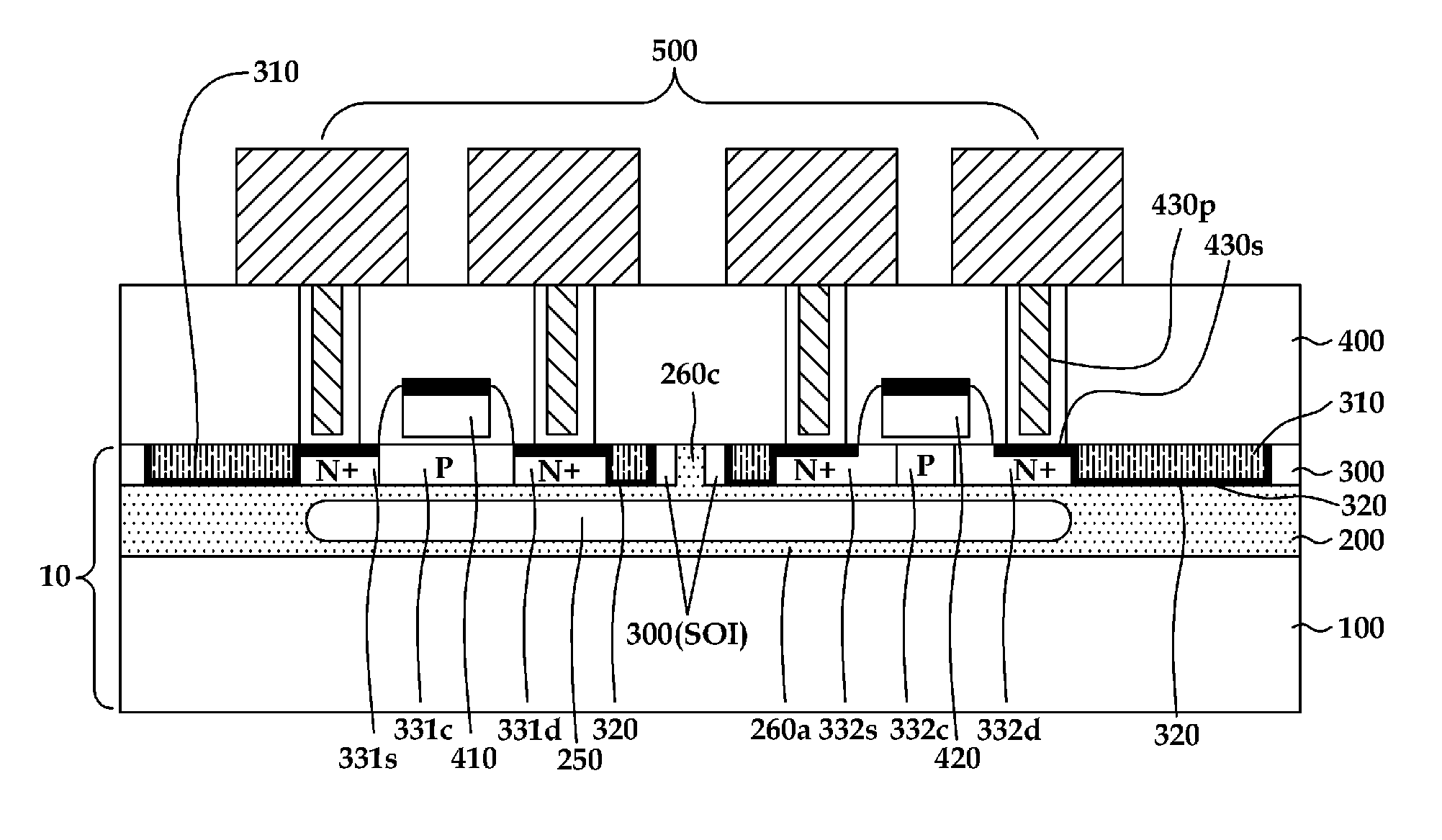
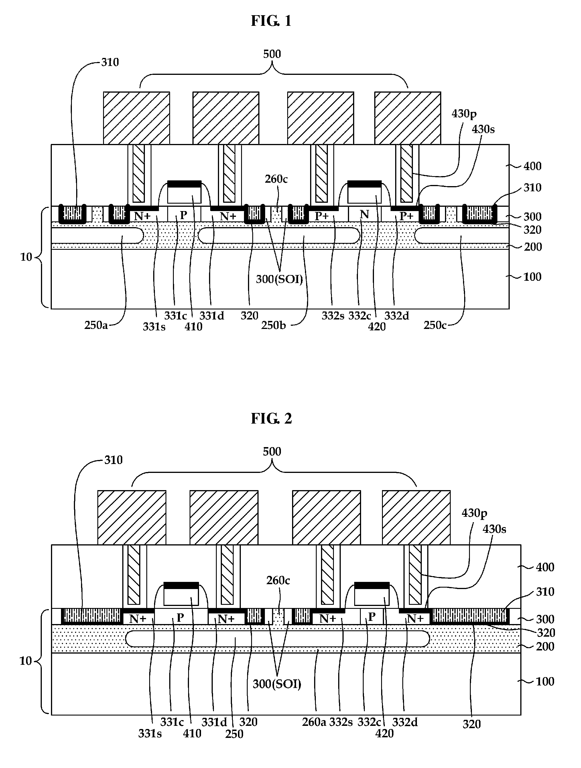
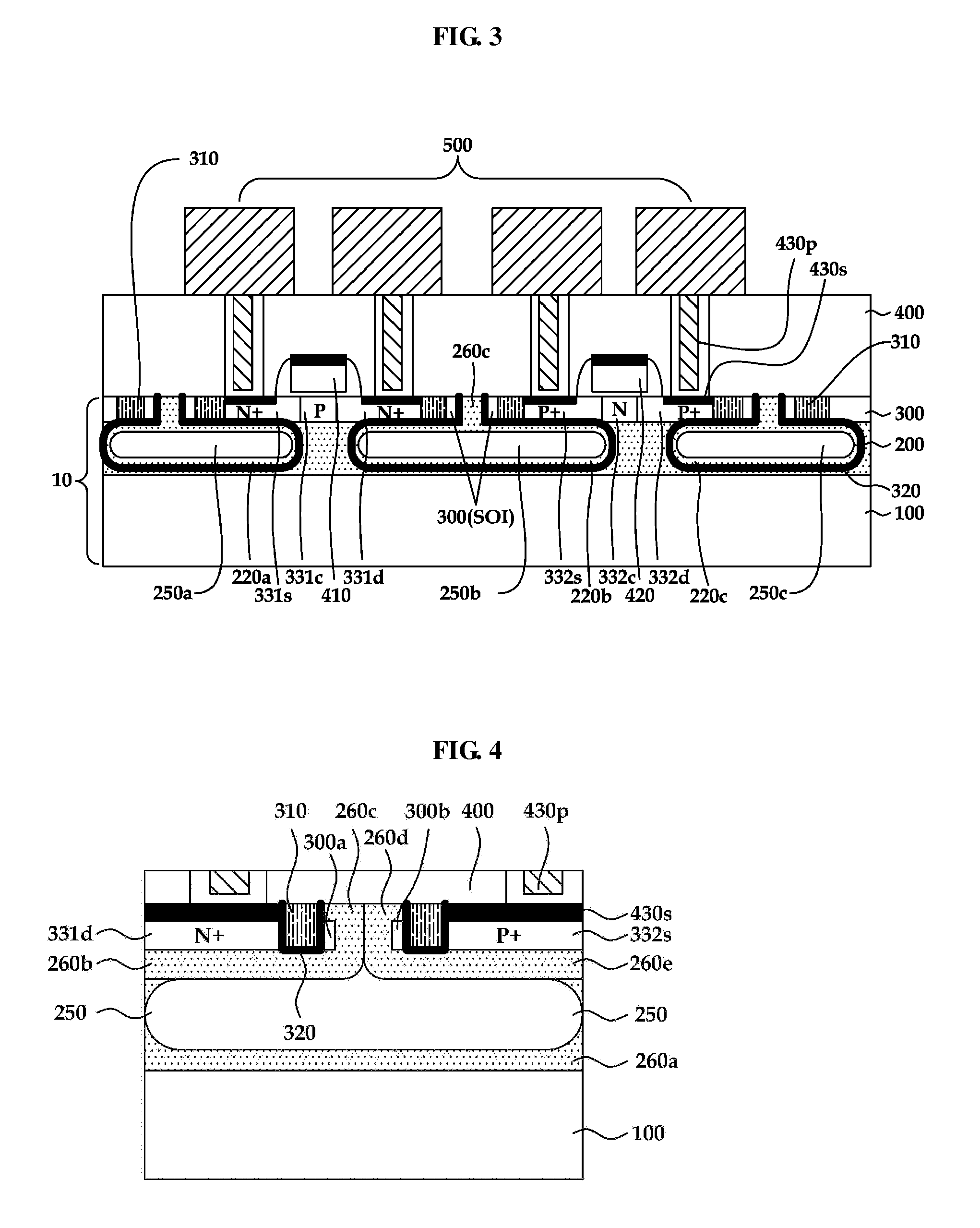
[0037]The following detailed description is provided to assist the reader in gaining a comprehensive understanding of the methods, apparatuses, and / or systems described herein. However, various changes, modifications, and equivalents of the systems, apparatuses and / or methods described herein will be apparent to one of ordinary skill in the art. The progression of processing steps and / or operations described is an example; however, the sequence of and / or operations is not limited to that set forth herein and may be changed as is known in the art, with the exception of steps and / or operations necessarily occurring in a certain order. Also, descriptions of functions and constructions that are well known to one of ordinary skill in the art may be omitted for increased clarity and conciseness.

[0038]The features described herein may be embodied in different forms, and are not to be construed as being limited to the examples described herein. Rather, the examples described herein have bee...


PUM


Abstract

A semiconductor device with voids within a silicon-on-insulator (SOI) structure and a method of forming the semiconductor device are provided. Voids are formed within a Buried Oxide layer (BOX layer) of the silicon-on-insulator (SOI) semiconductor to enhance a performance index of an RF-SOI switch. The semiconductor device with voids within a silicon-on-insulator (SOI) structure includes a semiconductor substrate; an insulating layer disposed on the substrate; a silicon-on-insulator (SOI) layer disposed on the insulating layer; a device isolation layer and an active area disposed within the SOI layer; one or more voids disposed within the insulating layer; and a sealing insulating sealing an opening of the void.

Description

CROSS-REFERENCE TO RELATED APPLICATIONS[0001]This application claims the benefit under 35 U.S.C. §119(a) of Korean Patent Application No. 10-2014-0065677 filed on May 30, 2014 in the Korean Intellectual Property Office, the entire disclosure of which is incorporated herein by reference for all purposes.BACKGROUND[0002]1. Field[0003]The following description relates to a semiconductor device with voids within a Silicon-On-Insulator (SOI) structure and a method of forming the semiconductor device. Voids are formed within a Buried Oxide layer (BOX layer) of the Silicon-On-Insulator (SOI) semiconductor and a performance index of a Radio Frequency-Silicon On Insulator (RF-SOI) switch is enhanced.[0004]2. Description of Related Art[0005]To improve a performance of the RF-SOI switch, i.e., a performance index (FOM) defined as (Ron*Coff), the product of a resistance value being on state resistance (Ron) and a capacitance value being an off state (Coff) of a switch device is required to be m...

Claims


Application Information

Patent Timeline
Patent Type & Authority Patents(United States)
IPC IPC(8): H01L29/06H01L27/12H01L21/764
CPCH01L21/764H01L27/1203H01L29/0649H01L21/84H01L21/02233H01L21/02255H01L21/02271H01L21/30604H01L21/308H01L21/31111H01L21/76283
Inventor HEBERT, FRANCOIS
Owner KEY FOUNDRY CO LTD
Why Eureka
Try Eureka