
Multi-register bank enhanced digital time delay integration using CMOS ROIC

Active Publication Date: 2016-06-21
HARRIS CORP
View PDF22 Cites 11 Cited by
  • Summary
  • Abstract
  • Description
  • Claims
  • Application Information

AI Technical Summary

Benefits of technology

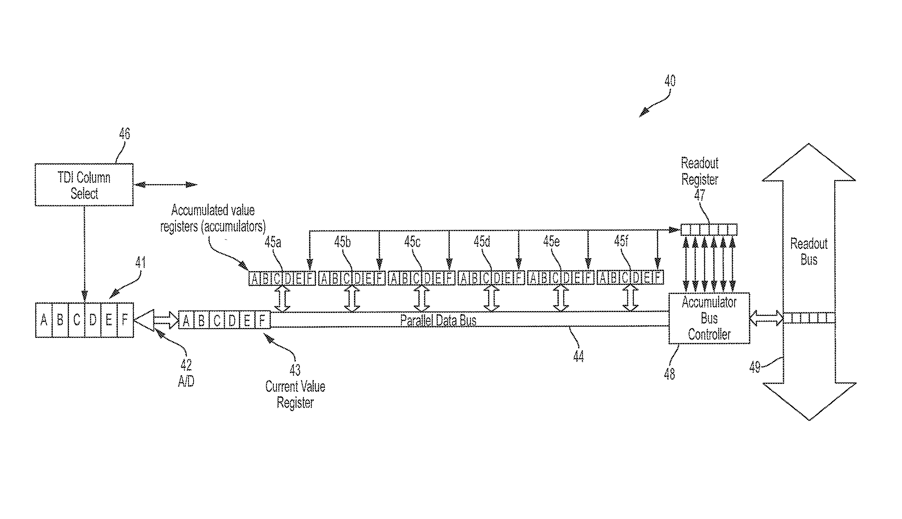
The present invention provides an integrated circuit for generating data of an image including a focal plane array (FPA) of sensing elements and a current value register for capturing pixel values. The integrated circuit includes an A / D converter for digitizing the captured image, and multiple accumulated value registers for storing pixel values from previous frames. The integrated circuit also includes a controller for selectively outputting pixel values from the current value register to the accumulated value registers. The accumulated value registers may store pixel values from different rows of the FPA. The integrated circuit can generate data of an image with improved accuracy and efficiency, and can also filter the image using multiple color bands.

Problems solved by technology

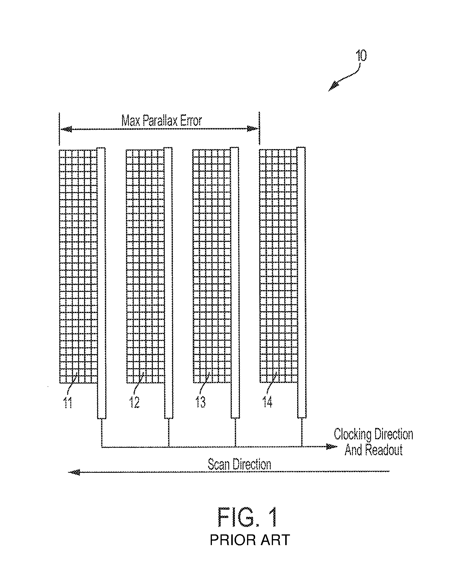
The in-track spatial offset between arrays, as shown in FIG. 1, can produce significant parallax error in remote sensing systems after aligning the pixels from the four bands to compensate for the offsets in the final image.
For large arrays the parallax error between the first and last filter band can make the imagery unusable.
In the example of FIG. 1, the in-track spatial offset between arrays would produce significant parallax error in remote sensing systems, because the pixels in the final image require spatial alignment.
For larger color arrays, the parallax error between the first and last color band can make the imagery unusable.

Method used


Image

  • Multi-register bank enhanced digital time delay integration using CMOS ROIC
  • Multi-register bank enhanced digital time delay integration using CMOS ROIC
  • Multi-register bank enhanced digital time delay integration using CMOS ROIC

Examples


Embodiment Construction

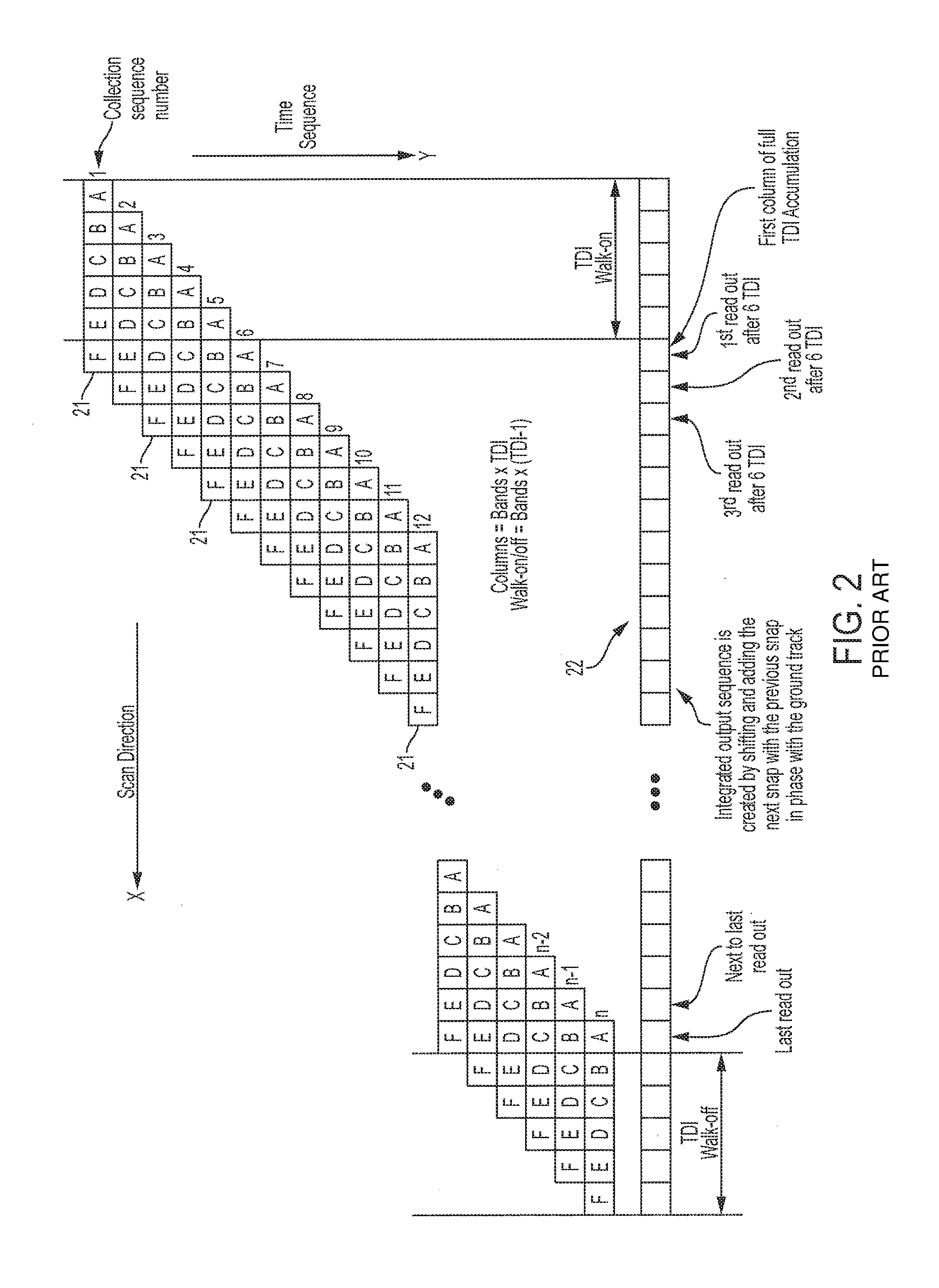
[0059]Conventional devices do not have the capability to accumulate multiple interlaced images when using a single accumulation ROIC per detector array. By having multiple accumulators attached to a single photo detector array, consecutive reads of a detector array (for example, a single row) is read into independent accumulation register banks. FIG. 3 illustrates an example of a concept of switching the source image, or image band color on a single array and collecting independent frames. Assuming a three color filter wheel (not shown) rotating at high speed in front of an image array, with each image array lasting so long as a given color of the wheel is in view, three independent images may be captured. If the frames are collected as the array is scanned in phase with the target, the image moves phase synchronously with the array.

[0060]As shown, FIG. 3 depicts collection sequence numbers (or frame numbers) 1-12, which are similar to the collection sequence numbers 1-12 of FIG. 2....


PUM


Abstract

An integrated circuit includes an array of pixels for capturing and processing successive image frames of a moving scene, the array including at least one row of pixels (inputs); and at least one current value register, in which the current value register is configured to store current pixel values captured from the array (inputs). Also included is at least one set of multiple accumulated value registers, in which each accumulated value register is configured to communicate with the current value register. Furthermore, there is included at least one readout register, in which the readout register is configured to communicate with the set of accumulated value registers. A controller is also included for shifting and summing the rows of pixels and outputting a summed column as a time delayed integrated (TDI) signal.

Description

FIELD OF THE INVENTION[0001]The present invention relates, in general, to digital time delay integration (TDI) scanning array devices using complimentary MOS (CMOS) technology. More specifically, the present invention relates to TDI functions built into an on-chip CMOS read-out integrated circuit (ROIC). The TDI functions use multiple accumulation registers for each row of pixels, thereby providing TDI accumulation for multiple spectral bands.BACKGROUND OF THE INVENTION[0002]Digital time delay integration (TDI) scanning array devices have been developed in recent years for applications in broad band (panchromatic) and multispectral imaging (MSI). These devices are typically constructed as 2-layer hybrid focal planes, comprised of a photo-detector layer and a Si-CMOS read-out integrated circuit (ROIC) that is bonded to the photo-detector layer. The ROIC performs a digital domain TDI function using high speed memory accumulators and shift registers that are configured to emulate an an...

Claims


Application Information

Patent Timeline
IPC IPC(8): H04N5/353H04N5/372H04N5/378
CPCH04N5/353H04N5/378H04N5/372H04N5/37206H04N25/70H04N25/768H04N23/125H04N25/711H04N25/71
Inventor SACCO, ANDREW P.NEWMAN, J. DANIEL
Owner HARRIS CORP
Learn More